
Back drilling is a special controlled-depth drilling process used in the production of multilayer boards to connect different layers, primarily applied in fields such as communication equipment, large servers, medical electronics, military, and aerospace.
★ Special Considerations for Back Drilling Design
✒︎ Determine the layers that require back drilling
Identify the specific layers that need back drilling during the PCB design phase, typically on internal signal layers or ground layers.
✒︎ Back drilling parameters
Select appropriate back drilling parameters based on design requirements and specifications, including the diameter, depth, and layers to be drilled through. These parameters are usually provided by RD based on the signal transmission requirements and electrical characteristics in the PCB design.
★ Definitions and Requirements for Common Terms in IPC Related to Back Drilling
💡Definition of back drilling
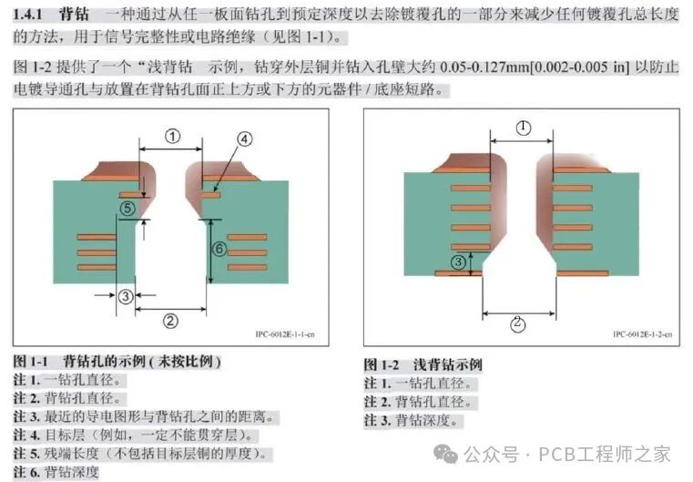 💡Definition of back drill stub
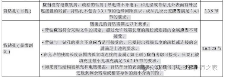
 💡Acceptance criteria
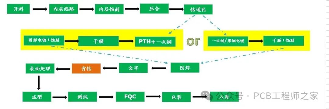
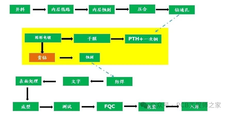
 ★ Production Process of Back Drilling Boards Each PCB manufacturer may have different operational processes for back drilling. Some may choose to perform back drilling after etching, which has the advantage of removing metal burrs and is suitable for through-hole back drilling design, but this process is slightly longer and may etch the internal copper foil. Another method is to perform back drilling after solder mask plug holes, which is more suitable for via hole back drilling and has a shorter process. The appropriate method depends on the manufacturer’s capabilities and the design conditions. The specific process flow is illustrated as follows: 💡Back drilling after solder mask
 💡Back drilling before etching
 ★ Processing Considerations
✒︎ Processing back drill holes
Use specialized back drilling equipment and drill bits to process the back drill holes for the required layers. Back drilling equipment typically uses back drill tools and depth control systems (automatically detecting depth) to control the depth and position of the back drilling.
✒︎ Removing back drilling debris
After completing the back drilling, it is essential to carefully remove the debris and residues generated in the back drill holes to ensure the quality and reliability of the back drill holes.
★ Back drilling capabilities and operational considerations
💡The conventional capability table is as follows:
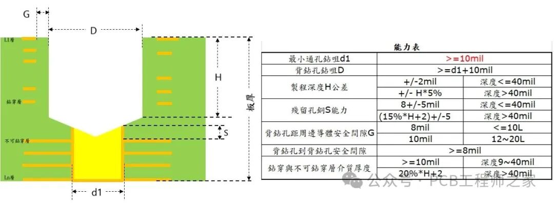 💡Shallow back drilling: back drilling depth and tolerance 0.1±0.05mm 💡Theoretical drilling depth: Drilling depth = (distance from the board surface to the top of the target layer) – (safety distance) – (drill tip length compensation). This calculation must be extremely precise and consider all compensation factors, which is a core control point in production. 💡First piece confirmation and process monitoring: The first board must undergo strict inspection, usually using micro-slicing (Cross-Section) to measure the actual drilling depth, check the stub residual length, safety distance, hole wall quality, and whether there is any damage to the inner layer.☆☆Key inspection items:✒︎Drilling depth accuracy & Stub length: Measure the stub length with a microscope to meet design requirements (usually target <0.15mm or shorter)✒︎Safety distance: Confirm that the distance from the bottom of the back drill to the copper foil of the target layer meets design requirements (>0.05mm)✒︎Concentricity: Measure the offset of the center of the back drill hole from the original through hole✒︎Hole wall quality: Check for resin dirt, burrs, and roughness.✒︎Inner layer damage: Confirm that non-target layers have not been damaged✒︎Outer layer connections: Check whether the edges of the back drill holes have damaged the outer layer traces or pads that need to be preserved 🚞🚃🚃🚃🚃🚃🚃🚃🚃🚃💨 The core challenge of the PCB back drilling process lies in precisely controlling the drilling depth (ensuring the elimination of stubs without damaging the target layer) and ensuring high concentricity. This relies on rigorous design specifications (especially drilling depth definitions and safety distances), high-precision equipment and drill bits, strict process control (especially drilling depth calculations, drill bit management, and parameter optimization), as well as reliable detection methods and excellent equipment, while fully considering DFM requirements during the design phase, which is key to successfully implementing the back drilling process.
This public account will continuously update content related to PCB/FPC design and manufacturing, please “follow” to avoid missing the content you need…
If this has been helpful to you, please bookmark➕share➕like, thank you!
Previous exciting content:
PCB Impedance Matching and Software Calculation
Current/Resistance/Capacitance/Inductance Calculation
Rigid-Flex PCB Issues and Solutions
FPC Design Issues and DFM Solutions
Common PCB Design DFM Traps
Basic Knowledge of PCB Materials (2)
Basic Knowledge of HDI (1)