Hello everyone, I am Jide Cheng.
Today I will share content related to the SPI protocol.
Table of Contents
-
Introduction
-
Table of Contents
-
First, let’s talk about UART
-
SPI Communication Protocol
-
Characteristics of SPI
-
Mode Numbers
-
Multi-Slave Mode
-
Advantages and Disadvantages
-
Programming Implementation
First, Let’s Talk About UART
I previously wrote an article on UART, the Universal Asynchronous Receiver-Transmitter protocol, which you can refer to as “An Easy-to-Understand UART Protocol Frame Format”; because UART does not have a clock signal, it cannot control when to send data, nor can it ensure that both ends receive data at exactly the same speed. Therefore, if both sides operate at different speeds for data transmission and reception, problems will arise.
To solve this problem, UART adds extra start bits and stop bits for each byte to help the receiver synchronize when the data arrives;
Both sides must also reach a consensus on the transmission speed (set the same baud rate, for example, 9600 bits per second).
A slight difference in transmission rates is not an issue because the receiver will resynchronize at the beginning of each byte. The corresponding protocol is shown in the figure below;
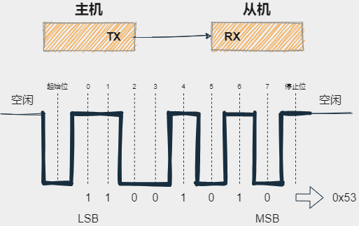
If you notice that the
11001010in the above figure does not equal 0x53, that is a detail. The serial protocol typically sends the least significant bit first, so the least significant bit is on the leftLSB. The low four bits of the byte are actually0011 = 0x3, and the high four bits are0101 = 0x5.
Asynchronous serial communication works well, but it incurs a lot of overhead due to the need for extra start bits and stop bits for each byte, as well as the complex hardware required for sending and receiving data.
It is not difficult to see that if the speeds set by the receiver and sender are inconsistent, the received data will be garbage (garbled).
Next, let’s discuss the SPI protocol and its advantages.
SPI Communication Protocol
So we wonder if there is a better serial communication method; compared to UART, SPI operates slightly differently.
SPI is a synchronous data bus, meaning it uses separate data lines and a separate clock signal to ensure perfect synchronization between the sender and receiver.
The clock is an oscillating signal that tells the receiver when to sample the signal on the data line.
The side generating the clock is called the master, while the other side is called the slave. There is always only one master (usually a microcontroller/MCU), but there can be multiple slaves (which will be detailed later);
The timing for data sampling can be on the rising edge (from low to high) or falling edge (from high to low) of the clock signal.
This depends on the configuration of the SPI;
The overall transmission can be divided into the following processes:
-
The master first pulls the
NSSsignal low to ensure data reception begins; -
When the receiver detects the clock edge signal, it immediately reads the signal on the data line, thus obtaining one bit of data (1
bit);Since the clock is sent along with the data, specifying the data transmission speed is not important, although devices will have a maximum speed they can operate at (we will discuss how to choose the appropriate clock edge and speed later).
-
The master sends data to the slave: the master generates the corresponding clock signal, and data is sent one bit at a time from the
MOSIsignal line to the slave; -
The master receives data from the slave: if the slave needs to send data back to the master, the master will continue to generate the predetermined number of clock signals, and the slave will send data through the
MISOsignal line;
The specifics are shown in the figure below;
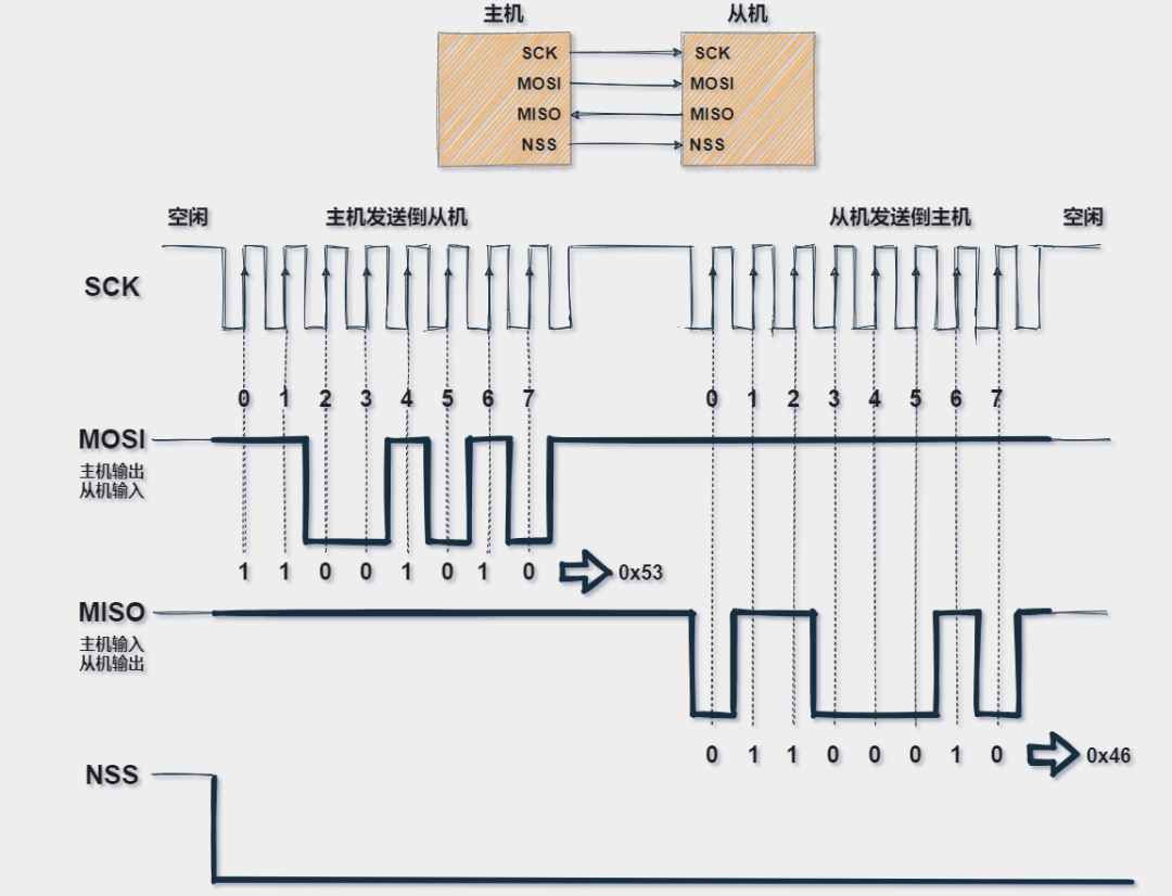
Note that SPI is “full duplex” (with separate send and receive lines), allowing data to be sent and received simultaneously. Additionally, the SPI receiving hardware can be a simple shift register. This is much simpler and cheaper than the complete UART required for asynchronous serial communication;
Characteristics of SPI
The SPI bus includes four logic lines, defined as follows:
-
MISO:
Master Input Slave Output(data from the slave); -
MOSI:
Master Output Slave Input(data from the master); -
SCLK:
Serial Clocksignal generated by the master and sent to the slave; -
SS:
Slave Selectsignal sent by the master to control which slave to communicate with, usually an active low signal.
Other manufacturers may follow different naming conventions, but they ultimately refer to the same meanings. Here are some common terms;
-
MISO may also be
SIMO,DOUT,DO,SDO, orSO(on the master side); -
MOSI may also be
SOMI,DIN,DI,SDI, orSI(on the master side); -
NSS may also be
CE,CS, orSSEL; -
SCLK may also be
SCK;
This article will use the following naming convention [MISO, MOSI, SCK, NSS]
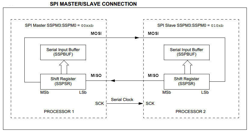
The figure below shows a typical SPI connection between a single master and a single slave.
Clock Frequency
The master on the SPI bus must configure and generate the corresponding clock signal at the start of communication. During each SPI clock cycle, full duplex data transmission occurs.
The master sends one bit of data on the MOSI line, which the slave reads, while the slave sends one bit of data on the MISO line, which the master reads.
Even for unidirectional data transmission, this order must be maintained. This means that something must actually be sent regardless of the data received! In this case, we refer to it as virtual data;
Theoretically, as long as it is feasible, the clock rate can be any rate you desire, of course, this rate is limited by the maximum system clock frequency that each system can provide and the maximum SPI transmission rate.
Clock Polarity CKP/Clock Polarity
In addition to configuring the serial clock rate (frequency), the SPI master device also needs to configure the clock polarity.
Depending on the naming conventions of hardware manufacturers, clock polarity is usually written as CKP or CPOL. Clock polarity and phase together determine how data is read, such as whether data is read on the rising edge or falling edge of the signal;
CKP can be configured as 1 or 0. This means you can set the default state (IDLE) of the clock to high or low as needed. Polarity inversion can be achieved through a simple logic inverter. You must refer to the device’s datasheet to set CKP and CKE correctly.
CKP = 0: Clock idleIDLEis low0;CKP = 1: Clock idleIDLEis high1;
Clock Phase CKE /Clock Phase (Edge)
In addition to configuring the serial clock rate and polarity, the SPI master device should also configure the clock phase (or edge). Depending on the hardware manufacturer, the clock phase is usually written as CKE or CPHA;
As the name suggests, the clock phase/edge refers to the specific phase or edge of the clock signal at which data is sampled;
CKE = 0: Sample on the first transition edge of the clock signalSCK;CKE = 1: Sample on the second transition edge of the clock signalSCK;
Summary of Clock Configuration
In summary of the above situations, the figure below summarizes all clock configuration combinations and highlights the actual sampling moments of the data;
The black line indicates the moments of data sampling;
The blue line indicates the SCK clock signal;
As shown in the figure below;
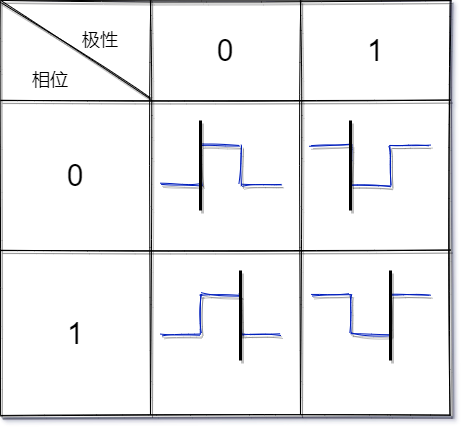
Mode Numbers
The configuration of the clock polarity and phase of SPI is usually referred to as SPI mode, and all possible modes follow the conventions shown in the table below;
| SPI Mode | CPOL | CPHA |
|---|---|---|
| 0 [00] | 0 | 0 |
| 1 [01] | 0 | 1 |
| 2 [10] | 1 | 0 |
| 3 [11] | 1 | 1 |
In addition, we should carefully check the mode table included in the microcontroller’s datasheet to ensure everything is functioning correctly.
Multi-Slave Mode
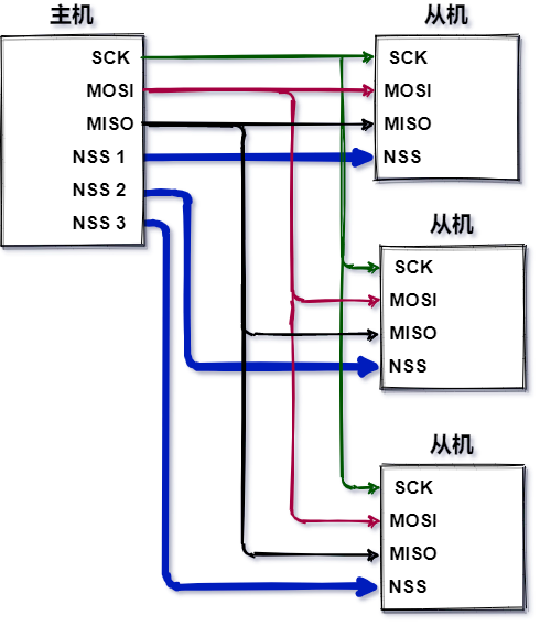
As mentioned earlier, the SPI bus must have one master and can have multiple slaves, so there are two specific methods to connect to the SPI bus:
First Method: Multiple NSS
- Typically, each slave requires a separate SS line.
- To communicate with a specific slave, the corresponding
NSSsignal line can be pulled low while keeping the otherNSSsignal lines high; if twoNSSsignal lines are pulled low simultaneously, garbled data may occur because both slaves may attempt to transmit data on the sameMISOline, ultimately leading to garbled received data.
The specific connection method is shown in the figure below;
Second Method: Daisy Chain

In the world of digital communication, the method of passing device signals (bus signals or interrupt signals) serially from one device to the next, continuously cycling until the data reaches the target device is called adaisy chain.
- The biggest disadvantage of the daisy chain is that because the signals are transmitted serially, if a device in the data link fails, the lower-priority devices below it will not be serviced;
- On the other hand, the further a slave is from the master, the lower its priority for receiving service, so it is necessary to arrange the priority of the slaves and set up a bus detector. If a slave times out, it should be short-circuited to prevent a single slave failure from causing the entire link to collapse;
The specific connection is shown in the figure below;
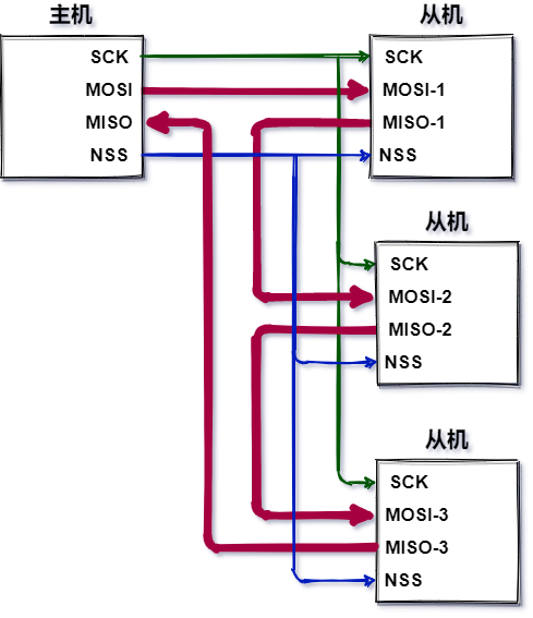
The red line indicates the direction of data flow;
Thus, the final data flow diagram can be represented as:
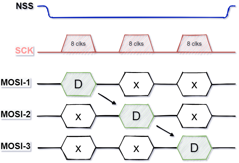
SCK is the clock signal, and 8clks indicates 8 edge signals;
Where D is data, and X is invalid data;
It is not difficult to see that the daisy chain mode fully utilizes the function of the SPI shift register, with the entire chain acting as a communication shift register, where each slave copies the input data to the output in the next clock cycle.
Advantages and Disadvantages
Advantages of SPI Communication
There are many reasons that make SPI stand out as a serial communication interface;
- Full duplex serial communication;
- High-speed data transmission rates.
- Simple software configuration;
- Extremely flexible data transmission, not limited to 8 bits; it can be of any size word;
- Very simple hardware structure. Slaves do not need a unique address (unlike I2C). Slaves use the master clock and do not require a precise clock oscillator/crystal (unlike UART). No transceiver is needed (unlike CAN).
Disadvantages of SPI
- No hardware slave acknowledgment signal (the master may send data without knowing if it is received);
- Typically supports only one master device;
- Requires more pins (unlike I2C);
- No defined hardware-level error checking protocol;
- Can only support very short distances compared to RS-232 and CAN bus;
Programming Implementation
Below is a portion of the HAL library code automatically generated by STM32’s CubeMX, which is relatively simple;
static void MX_SPI1_Init(void)
{
    hspi1.Instance = SPI1;
    hspi1.Init.Mode = SPI_MODE_MASTER;    // Master mode
    hspi1.Init.Direction = SPI_DIRECTION_2LINES; // Full duplex
    hspi1.Init.DataSize = SPI_DATASIZE_8BIT;  // Data size is 8 bits
    hspi1.Init.CLKPolarity = SPI_POLARITY_LOW;  // CPOL=0
    hspi1.Init.CLKPhase = SPI_PHASE_1EDGE;   // CPHA is the first transition edge of the data line
    hspi1.Init.NSS = SPI_NSS_SOFT;     // Software control of NSS
    hspi1.Init.BaudRatePrescaler = SPI_BAUDRATEPRESCALER_2;// 2 prescaler, 32M/2=16MHz
    hspi1.Init.FirstBit = SPI_FIRSTBIT_MSB;   // Send the most significant bit first
    hspi1.Init.TIMode = SPI_TIMODE_DISABLE;   // TIMODE mode disabled
    hspi1.Init.CRCCalculation = SPI_CRCCALCULATION_DISABLE;// CRC disabled
    hspi1.Init.CRCPolynomial = 10;     // Default value, invalid
    if (HAL_SPI_Init(&hspi1) != HAL_OK)    // Initialization
    {
        _Error_Handler(__FILE__, __LINE__);
    }
}

// Send data
HAL_StatusTypeDef
HAL_SPI_Transmit(SPI_HandleTypeDef *hspi,
                 uint8_t *pData,
                 uint16_t Size,
                 uint32_t Timeout);
// Receive data
HAL_StatusTypeDef
HAL_SPI_Receive(SPI_HandleTypeDef *hspi,
                uint8_t *pData,
                uint16_t Size,
                uint32_t Timeout);
I hope this helps you, see you in the next issue.
Recommended Reading:
How to Choose Pull-Up Resistor Values for I2C?
Electret Microphone (ECM) Circuit Design