This article delves into innovative methods for on-chip data transfer, exploring how embedded engineers can strategically design FPGA systems to alleviate the memory wall issue and fully unleash the potential of these powerful devices.
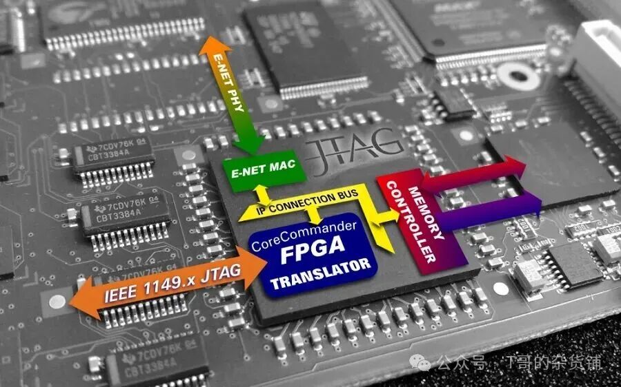
For embedded engineers, Field Programmable Gate Arrays (FPGAs) represent a powerful paradigm for accelerating compute-intensive applications. Their inherent parallelism and reconfigurability offer unparalleled opportunities for custom hardware design, significantly enhancing performance and energy efficiency compared to traditional processors. However, as FPGA processing capabilities continue to soar, a familiar adversary is increasingly coming to the forefront: the “memory wall.” This ubiquitous bottleneck phenomenon—where computation speeds far exceed memory data access rates—is threatening the core advantages of FPGAs, becoming a critical challenge that needs to be addressed.
The memory wall is not a new phenomenon in computing, but its manifestation in FPGAs presents unique complexities. Unlike CPUs, which have complex cache hierarchies and powerful memory controllers, FPGAs typically rely on more direct, application-specific data transfer strategies. This extreme flexibility that makes FPGAs so attractive, if not carefully managed, can lead to highly fragmented and inefficient data access patterns. This article delves into innovative methods for on-chip data transfer, exploring how embedded engineers can strategically design FPGA systems to alleviate the memory wall issue and fully unleash the potential of these powerful devices.
Understanding FPGA Memory Architecture
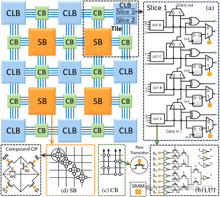
Before exploring solutions, it is crucial to understand the internal memory architecture of FPGAs. Modern FPGAs typically feature a multi-level memory hierarchy, with each level having unique characteristics:
- Registers: The fastest and smallest form of storage, directly integrated into logic units. They are ideal for immediate data operations and temporary result storage within a single clock cycle.
- Block RAM (BRAM): Dedicated on-chip synchronous RAM modules that offer higher capacity and significantly lower latency compared to external memory. BRAM is highly configurable (e.g., single-port, dual-port, simple dual-port, FIFO) and serves as the primary storage unit for on-chip data buffering, lookup tables, and small datasets. Its distributed nature within FPGA architecture is a key advantage.
- Ultra RAM (URAM): (Specific to Xilinx UltraScale+ FPGAs) A high-density storage module with larger capacity, designed for applications requiring more on-chip storage than BRAM while still providing extremely high bandwidth.
- External Memory Interfaces (DDR, HBM): Connect FPGAs to off-chip DRAM modules (such as DDR4 or the increasingly popular High Bandwidth Memory HBM). These interfaces provide maximum storage capacity but come with significantly higher latency and lower bandwidth compared to on-chip memory.
The core of the memory wall issue in FPGAs stems from the vast speed disparity between on-chip computation and external memory access. Even within the FPGA, inefficient data transfer between distributed BRAMs or from BRAM to processing units can become bottlenecks. Therefore, optimizing on-chip data movement is crucial.
Innovative Solutions for On-Chip Data Movement
To effectively tackle the memory wall issue, embedded engineers are adopting a range of innovative strategies that go beyond simple data buffering. These methods focus on maximizing data reuse, minimizing external memory access, and intelligently coordinating data flow across the FPGA architecture.
Dataflow-Centric Design and Pipelining Techniques
One of the most powerful paradigms for data transfer within FPGA chips is dataflow programming. Unlike traditional imperative execution, dataflow design models computation as a network of interconnected processing elements (PEs), where data “flows” from one operation to the next.
- Deep Pipelining: FPGAs excel at pipelined processing, breaking complex computations into a series of sequential stages. Each stage processes different blocks of data simultaneously, significantly enhancing throughput. By carefully designing the pipeline, engineers can ensure that data continuously flows through the processing units, effectively masking memory latency. This requires strategically placing registers between pipeline stages to maximize clock frequency and avoid combinational logic paths that span large areas of the FPGA.
- Stream-Based Architectures: Many modern High-Level Synthesis (HLS) tools advocate for stream-based data transfer, treating data as a continuous flow moving through FIFO buffers between functional units. This approach is inherently suited for pipelined designs, reducing explicit memory addressing requirements and maximizing data locality. Data is consumed immediately upon generation, minimizing idle cycles.
- Producer-Consumer Model: This aligns naturally with dataflow processing. Functional blocks are designed as producers or consumers of data, with FIFOs serving as decoupling buffers between them. This design allows functional blocks to operate asynchronously, accommodating different processing rates and avoiding stalls caused by memory access delays.
Advanced On-Chip Memory Architectures
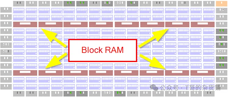
In addition to simply using BRAM, new architectural patterns are emerging to optimize their utilization:
- Memory Grouping and Partitioning: Designers can distribute data across multiple smaller BRAMs (memory grouping) rather than using a single large memory block. This architecture supports parallel access to different storage bodies, significantly enhancing effective memory bandwidth. For instance, when an algorithm requires simultaneous access to multiple data streams, allocating independent BRAMs for each data stream can completely eliminate access conflicts. Careful data layout and addressing design are crucial in this scenario.
- Compute-in-Memory (CiM) Paradigms: Although not yet mainstream in the FPGA domain like dedicated ASICs, the concept of “compute-in-memory” is gaining attention. This technology integrates or closely deploys computational logic next to storage units. For FPGAs, highly localized computation can be achieved by designing small dedicated processing units near BRAM, avoiding significant data movement overhead. For example, the “CoMeFa RAM” concept integrates processing elements within BRAM to support parallel compute-in-memory operations.
- Buffer Memory and Chunking Techniques: For iterative algorithms, repeatedly loading entire datasets from external memory is highly inefficient. Buffer memory, explicitly managed by designers, can store frequently accessed subsets of data. Chunking techniques divide large datasets into smaller, more manageable “chunks” that can be placed in on-chip memory. Computation is then performed on these data chunks, minimizing external memory access. Once one data chunk is processed, the next can be loaded.
High Bandwidth Memory (HBM) Integration
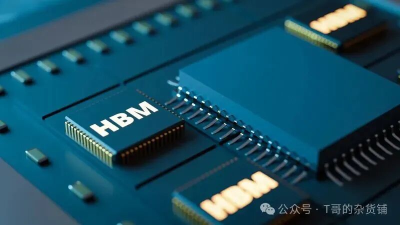
The advent of FPGAs integrated with High Bandwidth Memory (HBM) stacks has brought revolutionary changes to addressing the memory wall issue. Compared to traditional DDR interfaces, HBM offers significantly higher bandwidth and lower latency due to its 3D stacked architecture and wide interface.
- Utilizing HBM Channels: HBM typically provides multiple independent memory channels. By mapping different data streams or large data structures to different HBM channels, FPGA designs can be customized to leverage this parallelism. For inherently data-intensive applications such as deep learning inference and high-performance computing, this large-scale parallel access can significantly reduce memory access bottlenecks.
- Co-Optimizing HBM with On-Chip Memory: The true power of HBM is unleashed when it is intelligently co-optimized with FPGA on-chip memory. HBM can serve as the high-speed “main memory” for the FPGA, while BRAM and URAM act as ultra-fast caches or temporary storage to meet immediate data needs. This multi-level memory hierarchy (with HBM filling the gap between external DRAM and on-chip SRAM) becomes a powerful tool in tackling the memory wall challenge.
Scalable On-Chip Networks (NoC)
As the complexity of FPGA designs increases and more heterogeneous processing units are integrated, simple bus-based communication architectures quickly become performance bottlenecks. On-chip network (NoC) architectures provide a scalable packet-switched communication infrastructure for FPGAs.
- Structured Data Flow Transmission: In large-scale FPGAs, NoC provides a more structured and predictable data transmission method between different IP modules, processing clusters, and memory controllers. This is particularly important for multi-die FPGAs (small chip groups), as communication across Super Logic Regions (SLRs) incurs significant latency and resource overhead. The increasingly popular hardened NoCs in advanced FPGAs can provide optimized low-latency paths.
- Congestion Avoidance and Load Balancing: NoC employs routing algorithms and flow control mechanisms to manage communication traffic and avoid congestion, maintaining more stable data transmission latencies even under high loads. This sharply contrasts with traditional shared bus architectures, which experience bottlenecks as the number of communication nodes increases.
- Enabling Heterogeneous Integration: As FPGAs are often integrated into heterogeneous systems (such as working alongside CPUs and GPUs), on-chip networks facilitate efficient data exchange both within the FPGA and between external components, becoming a key pillar in complex system-on-chip designs.
Resource Scheduling and Data Path Optimization
In addition to architectural choices, fine-grained resource scheduling and data path optimization at the RTL level are still crucial for achieving efficient on-chip data transfer.
- Fine-Grained Gating and Buffering: When used judiciously between functional units, clock gating and explicit buffering (FIFO) can regulate data flow, prevent blocking, and ensure data arrives precisely when needed. This can minimize wasted cycles due to data not being ready.
- Leveraging Data Locality: By optimizing the layout of computation and data storage, the data reuse rate of on-chip memory can be maximized, thereby reducing the frequency of data retrieval from slow external storage. Common practices include restructuring algorithms to prioritize processing highly localized small datasets before gradually advancing. Loop blocking and data chunking are classic applications of this concept.
- Merging Memory Accesses: Aggregating scattered memory access requests into larger contiguous burst transfers can significantly enhance efficiency (especially when interacting with external memory interfaces), effectively reducing the overhead associated with processing multiple small transactions.
- Adaptive Data Migration Strategies: Static data migration strategies may not be optimal for certain applications. Researchers are exploring adaptive approaches that can dynamically adjust data migration patterns based on runtime states or workload characteristics.
Case Studies and Future Directions
The impact of these innovative methods is evident in various high-performance computing and data-intensive applications. For instance, in the neuromorphic computing domain, FPGAs are being explored as brain-like artificial intelligence platforms. In this scenario, efficient memory utilization and rapid on-chip data transfer are crucial for handling vast amounts of synaptic weights and activation values. Research in this field actively investigates how to reduce DRAM access through near-memory processing and how to enhance SRAM with ROM caching to alleviate the memory wall issue.
In the deep learning inference scenario, FPGA accelerators heavily rely on highly optimized on-chip memory architectures and dataflow pipelines to achieve high throughput and low latency. Memory chunking techniques, fine-grained weight quantization, and dataflow transmission through cascaded processing units are essential for continuously supplying computation units and avoiding stalls. Some designs even implement “all-on-chip” solutions for small models, storing input images and hidden layer feature maps directly in FPGA memory, thereby completely eliminating external DRAM access.
Looking ahead, the development of FPGA storage solutions may continue to advance in several directions:
- Further Integration of Emerging Storage Technologies: While High Bandwidth Memory (HBM) is a significant breakthrough, future FPGAs may directly integrate other non-volatile memories (such as Resistive RAM (ReRAM) and Phase Change Memory (PCM)) within the package or even on-chip, further blurring the lines between computation and storage.
- Smarter Memory Controllers: More intelligent (and possibly AI-driven) memory controllers will play a critical role, capable of predicting data access patterns and proactively prefetching data.
- More Advanced Abstractions and Tools: As lower-level optimizations become increasingly complex, High-Level Synthesis (HLS) tools will need to evolve to automatically infer and implement precise data movement strategies from high-level descriptions in C/C++/OpenCL, thereby alleviating the burden on embedded engineers.
- Open Source Hardware and Standards: Developing open standards and open-source IP cores for on-chip interconnects and memory interfaces will help drive further innovation and enhance interoperability.
Conclusion: Building a Data-Centric Engineering Future
The memory wall remains a long-standing challenge in FPGA design, but it is by no means an insurmountable barrier. By adopting innovative on-chip data transfer solutions—from dataflow-centric designs and advanced memory architectures to integrated HBM memory and robust on-chip network solutions—embedded engineers can build efficient and high-performance FPGA systems. The key lies in shifting the design mindset from merely “computing data” to “intelligently transferring data to enable computation.” This data-centric way of thinking, combined with a deep understanding of FPGA memory hierarchies, is crucial for unlocking the full potential of these multifunctional devices.