
Introduction
During the FPGA development process, it is common to encounter situations where data needs to be cached for later use. Typically, there are two solutions: RAM and FIFO. However, using FIFO has two limitations:
- There is a fixed delay of at least 3 clock cycles between FIFO output and input, and it cannot be sent out in 1 clock cycle;
- FIFO must operate in a first-in, first-out manner;
In contrast, using RAM for caching can overcome these two limitations, achieving a delay of only 1 clock cycle between output and input, and allowing for output selection without adhering to the first-in, first-out rule.
Recommended RAM Solutions
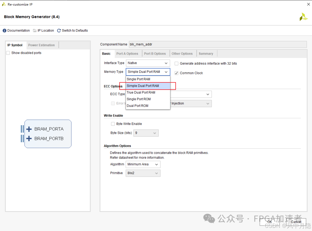
Xilinx’s block memory IP has 5 types, of which 3 are RAM, as shown in the image above.
In most cases, I personally recommend the second option highlighted in the box: simple dual port RAM mode.
The advantage over the first option (single port RAM) is that the read and write addresses are separate, allowing the output data to be unaffected by the input address;
The advantage over the third option (true dual port RAM) is that the read and write timing is simpler, requiring fewer control signals for read and write enables;
Recommended Settings for RAM Usage
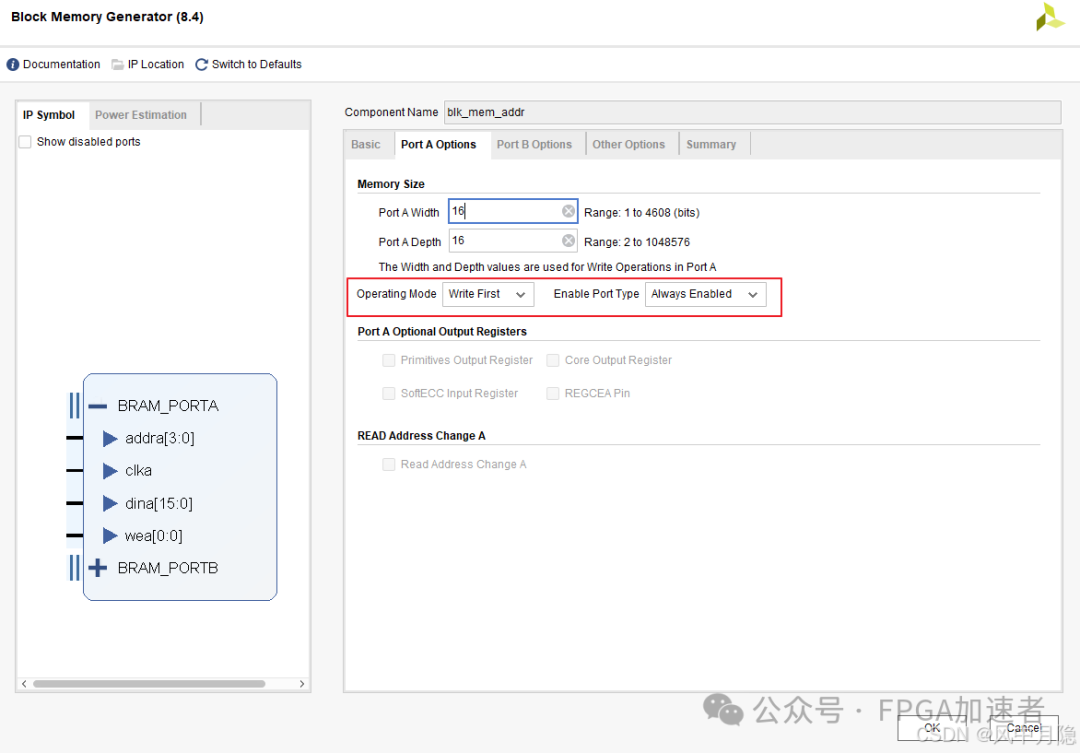
Settings for Port A as shown in the red box below:
-
write first: This ensures that when the read and write addresses are the same, the write operation occurs before the read, maintaining the first-in, first-out order;
-
always enabled: This ensures that when storing data, only one write enable (wea) needs to be controlled, reducing the number of control signals;
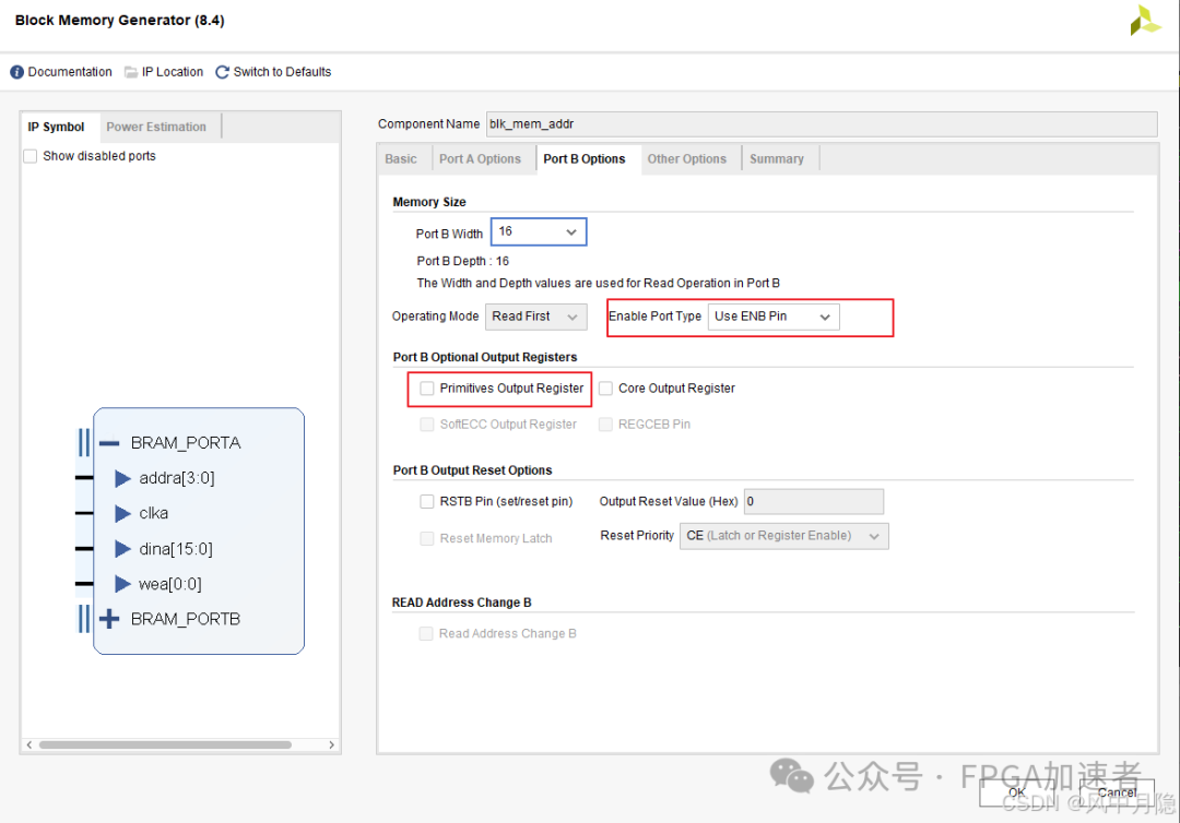
Settings for Port B as shown in the red box below:
use ENB pin: This ensures that when an ENB signal is given, one data output is produced, and when not given, the output remains unchanged, aligning with conventional human thinking;
primitives output register: do not check This ensures that the delay between the read enable and the read output data is 1 CLK; if checked, it becomes 2 CLK.
Keep the remaining pages at default settings.
If this article has been helpful to you, feel free to like, share, bookmark, or comment to let more people see it. Your support would be greatly appreciated.
If you have any questions about the content of the article, please describe your issues clearly, leave a comment, or send me a private message, and I will respond when I see it.

FPGA practitioners are welcome to follow the WeChat public account FPGA Accelerator for more exciting content.
#Previous Articles
Why can’t your ZU4xDR RF-DAC be configured to the officially stated 10GSPS sampling rate? Online update and reloading of FPGA bit for ZYNQ using slave select MAP solutionWhat points should be noted for clock synchronization with multiple MHC7044 clock chips?