1. The addressing art presented in Chapter 27 of the ATMEGA328 chip datasheet.
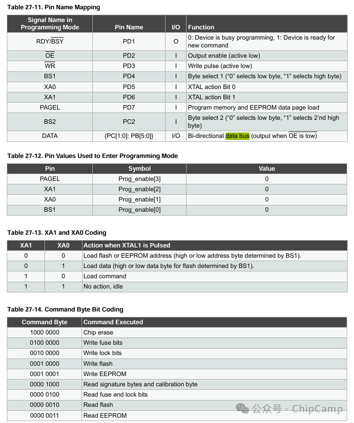
—- Three key terms: Data bus!! Command!! Address!!
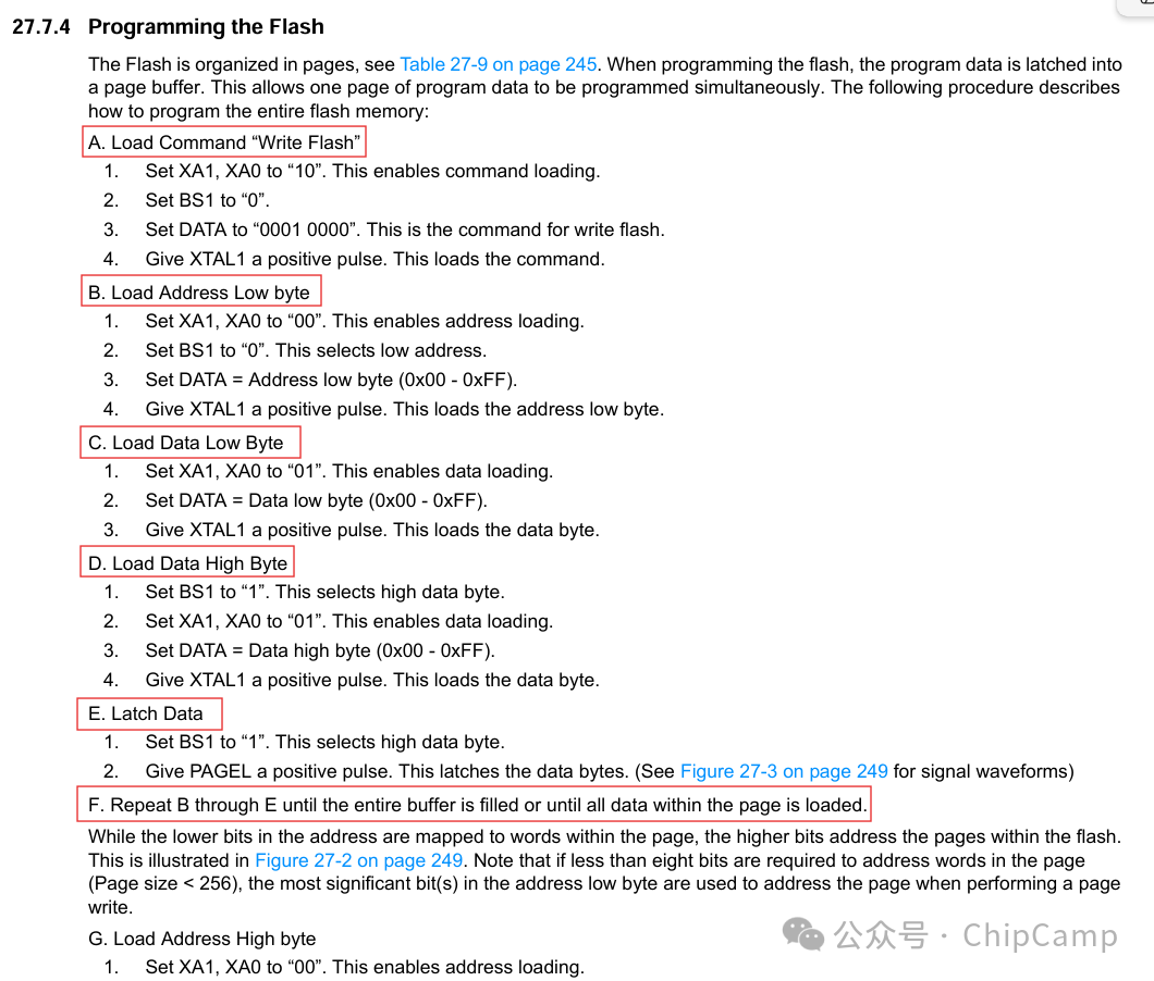
—- An exciting message semantic process of {Command + Address + Data + Latch Data}!! Further explanation combined with waveform diagrams.
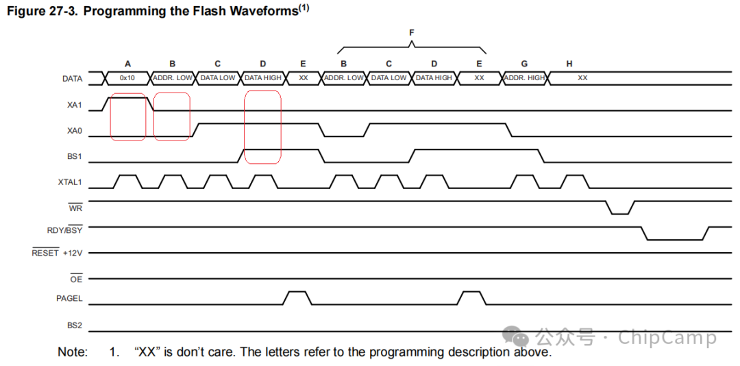
—- The first red box indicates that under the control signals of XA=10 && BS1=0, the 8-bit DATA signal transmits Command=0x10, which signifies Write Flash.
—- The second red box indicates that under the control signals of XA=00 && BS1=0, the 8-bit DATA signal transmits AddrLow.
—- Before the third red box, at XA=01, the 8-bit DATA signal transmits DataLow.
—- The third red box indicates that under the control signals of XA=01 && BS1=1, the 8-bit DATA signal transmits DataHigh.
—- After the third red box, while maintaining BS1=1 in the previous DataHigh state, the 8-bit DATA signal transmits DontCare (i.e., the xx in the diagram), and the hardware circuit completes data latching at this clock edge (excluding the xx value).
2. Summary.
—- Using an 8-bit DATA signal to sequentially transmit {Command + Address + Data + DataLatchInd} represents a state between parallel and serial buses! The 8-bit DATA signal width ensures that 8 bits or 1 byte of data are transmitted in parallel during each clock cycle, which is parallel and clock-controlled. This synchronous clock control is manifested in the signals of XA and BS1, or more precisely, in the out-of-band control signals of the data signals. Meanwhile, the sequential transmission of {Cmd + Addr + Data + xx} on this 8-bit DATA signal is clearly serial. This forms a unique Paradigm 1, corresponding to two different paradigms: parallel bus and serial bus. As follows.
—- Paradigm 1: Serial {Cmd + Address + Data} byte stream on byte-level parallel data signals with out-of-band synchronization signal control.
—- Paradigm 2: All {Ctrl + Address + Data} in parallel (purely) parallel bus. If Address and Data are 64 bits, a total of 128 bits of width is required.
—- Paradigm 3: Purely serial bus represented by SERDES, converting parallel bus to {Data-only Serial Bus}, without any out-of-band control signals for synchronization, relying instead on SERDES to recover the clock from the {Data-only Serial Bus} and to recover {Cmd + Address + Data} based on physical encoding such as preambles and end symbols.
—- Compared to the completely parallel Paradigm 2, Paradigm 1 significantly reduces data width! It reduces the 128 lines of Addr + Data in the example of Paradigm 2 down to 8. Even if control lines like XA and BS1 are added, it still reduces the count by a factor of ten.
—- Compared to the completely serial Paradigm 3, Paradigm 1 reduces the complexity of high-speed SERDES while maintaining the simplicity of synchronous read/write (synchronous control signals under the same clock control).
—- It perfectly demonstrates a form that lies between parallel bus Address and serial bus Address!
3. The work of computer scientist Bill Dally, “Digital Design System Method”.
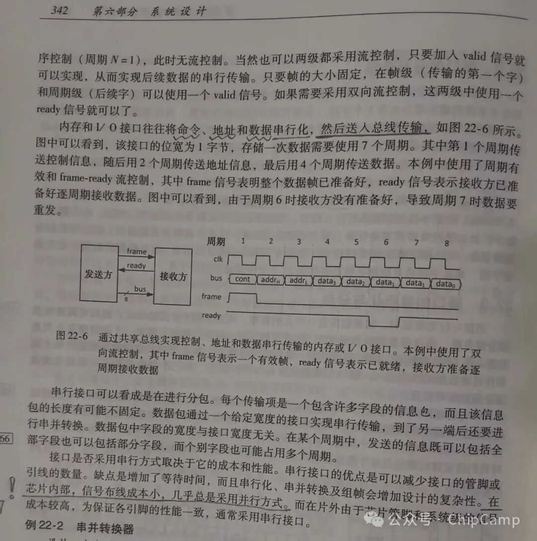
—- When designing interfaces, fields are typically divided into control fields, address fields, and data fields. Control fields determine what operation to perform, address fields determine where to perform the operation, and data fields provide (or receive) the data related to the operation.
—- Memory and I/O interfaces often serialize commands, addresses, and data, and then send them into the bus for transmission.
—- As shown in Figure 22-6, the data width of this interface is 1 byte, requiring multiple cycles to store data at once, where the first cycle transmits control information, followed by 2 cycles for address information, and finally 4 cycles for data. This example uses cycle-valid and frame-ready flow control.
—- Inside the chip, signal wiring costs are low, and parallel methods are almost always used. However, outside the chip, due to the high cost of chip pins and system-level signals, serial interfaces are typically used.
—- Given the abundance of internal resources, a fully parallel bus is usually a good solution. However, when data outside the chip or within the chip has already been serialized, it is best to use a serial bus like that in Figure 22-6, allowing data transactions to complete in several cycles, which can reduce the number of pins or avoid the cost of adding serial-parallel conversion.
—- All of the above are original texts from Bill Dally! They excellently explain this bus state located between parallel and serial buses! They completely match the examples seen in the ATmega328 datasheet! This is also the reason for supplementing this article, as the summaries seen from the “bottom-up” after observing the ATmega328 and the “top-down” reading of Bill Dally’s book are completely consistent, and this surprise inspired the recording and memorization of this article.
—- Who is Bill Dally? His full name is William J Dally, the Chief Scientist at NVIDIA and a professor for over 30 years in the United States. In addition to this book, “Digital Design System Method”, he also has a classic book titled “Principles and Practices of Interconnection Networks”.
—- The text above contains a lot of information worth referencing. For example:
—- The data width is 1 byte, consistent with the storage control of the ATmega328 mentioned above.
—- The order of information transmission, first control information (command), then address, and finally data, is also consistent with the example of the ATmega328.
—- Additionally, the frame-ready flow control is a common pattern, with many base classes in Chisel language generating ready-valid signals, and derived bundles inheriting the ready-valid signals defined by the base class as a certain interface paradigm. Of course, this is not closely related to the Address paradigm discussed in this article, but it is worth noting here.
—- It is best to use a serial bus like that in Figure 22-6, allowing data transactions to complete in several cycles, which can reduce the number of pins or avoid the cost of adding serial-parallel conversion. // This sentence perfectly matches the method used by the ATmega328, as a fully parallel approach would result in too many pins. If a purely serial approach is taken, the cost of SERDES serial-parallel conversion is high, as the clock recovery during asynchronous reception and decoding data field boundaries from pure data bits are extremely complex. The intermediate method shown in the ATmega328 datasheet, which is summarized in this article:
—- Paradigm 1: Serial {Cmd + Address + Data} byte stream on parallel {8 bits} data signals with out-of-band synchronization signal control.
—- Furthermore, the surprise of rereading this book lies in its emphasis on the two key terms: chip + system. For example, in the preface, the author states: The purpose of this book is to teach college students to understand and design digital systems. Our original intention in writing this book is that there is currently no book on the market that introduces digital design from a system-level perspective. It is impossible to cultivate students who can design GPUs with 3 billion transistors. We will adopt a simple approach to introduce it without getting bogged down in details.
—- Chapter 22, “Interfaces and System-Level Timing”, belongs to system design in this book. This reflects the author’s writing characteristic of system.
—- The title of Section 2.2 in the book is: Digital systems are constructed from chips and circuit boards. The first sentence of the following text elaborates: Modern digital systems are realized by connecting standard integrated circuits and custom integrated circuits on circuit boards, which are then interconnected through connectors and cables.
—- This is almost identical to what this article, this series, and even this account have focused on so far! The term chip system in the title of this article emphasizes a system composed of chips! This series specifically mentions that this system includes the concept of SoC/SiP/SoB as representatives of systems. The essence of this article is also the interface between CPU chips and I/O peripherals, considering the system. Along with the previous memory, they together form the three core components of chip systems represented by SoC/SiP/SoB —- CPU, memory, and peripherals.
4. Mr. Yang Zhenning emphasizes inductive reasoning and permeable learning methods.
—- As this article is written to this point, I again think of Mr. Yang Zhenning’s emphasis on inductive reasoning and permeable learning methods.
—- As mentioned earlier: because the summaries seen from the “bottom-up” after observing the ATmega328 and the “top-down” reading of Bill Dally’s book are completely consistent, this surprise inspired the recording and memorization of this article.
—- The summaries seen after observing the ATmega328 and those seen in Bill Dally’s work are exactly the former from phenomenon/reality products to paradigm summaries, and the latter from theory/book to phenomenon/reality products (explanation). The former is roughly equivalent to moving from phenomenon to theory, while the latter is roughly equivalent to moving from theory to phenomenon.
—- Mr. Yang’s inductive reasoning and permeable learning methods can be found online. I hope to see a systematic compilation of his speeches published as a book. Currently, I have the 5th edition of “The Biography of Yang Zhenning” at hand, but I have not found these two terms, which may not have included his speeches on permeable learning methods. However, I still see similar viewpoints in the book. I remind myself to pay attention to Mr. Yang’s new book, TBD.
<<<<<<<<END>>>>>>>>
Abstract: This article explores a unique addressing paradigm presented in the ATMEGA328 chip datasheet, which lies between parallel and serial buses. By sequentially transmitting commands, addresses, and data through an 8-bit data signal, combined with out-of-band synchronization control signals, efficient data transmission is achieved. The article summarizes this design as Paradigm 1 and compares it with fully parallel Paradigm 2 and purely serial Paradigm 3. It also references the work of computer scientist Bill Dally, confirming the advantages of this design in reducing pin counts and avoiding complex serial-parallel conversions. Finally, the article mentions Yang Zhenning’s inductive reasoning and permeable learning methods, emphasizing the bidirectional verification process from practice to theory and theory to practice.
Copyright Statement: This article is an original work by CSDN blogger “ChipCamp”, following the CC 4.0 BY-SA copyright agreement. Please include the original source link and this statement when reprinting. Original link:
https://chipcamp.blog.csdn.net/article/details/155314427