
In ASIC or FPGA system design, we often encounter the issue of data transmission across multiple clock domains, and timing issues become increasingly severe as the system grows more complex.
Cross-clock domain processing technology is a crucial part of IC design. We need to learn and apply some common processing methods to enhance the stability of circuit operation and make the entire system more robust.
Considering the ASIC design scenario, to meet the system functionality requirements, the entire system consists of different functional blocks, such as:
-
Processor
-
Memory
-
Floating Point Engine
-
Memory Controller
-
Bus Interface
-
High-Speed Interface
For instance, if we consider the operating frequency of the processor and memory as 500MHz, the floating point engine with a memory controller operating at 666.66MHz, and the bus and high-speed interfaces operating at 250MHz, then this design has multiple clocks and is viewed as a design with multiple clock domains.
01
Common Methods for Multi-Clock Domain Design
As mentioned earlier, the processing issues of multiple clock domains affect data integrity during the transmission of data and control signals. The following strategies are useful during the ASIC design phase.
-
Try to develop strategies for optimizing data and control paths.
-
Try to create multiple clock domain groups to define strategies.
-
When transmitting control signals between multiple clock domains, try to use synchronizer strategies.
-
Try to use FIFO and cache data path synchronizers to improve data integrity.
Now let’s discuss important cross-clock processing problems and strategies and their use in multi-clock domain designs.
02
What Problems Exist in Multi-Clock Domain Design
If we consider a moderately sized gate design or a processor core operating with a single clock, it may encounter timing violations during the layout phase due to additional interconnect delays. However, this design may be adjusted to meet timing and performance through architecture, RTL, synthesis, and tool-based optimizations.
Now consider the design that requires multiple clocks as shown in the diagram; let’s try to understand the problems within the design.
1. Data integrity is a major issue due to multiple clock domains, and the design needs to undergo data integrity checks.
2. Flip-flops at the clock domain boundary that do not use synchronizers will have metastability issues due to setup and hold violations.
3. The design will have timing violations and will be difficult to enforce that the timing circuit outputs enter a valid legal state.
Let’s understand the above content with a timing circuit that has multiple clock domains. Due to the difference in arrival times between clk1 and clk2, the flip-flop in the second clock domain will have setup and hold violations, meaning the flip-flop output data_out will be in a metastable state. The reason is that the q output of clock domain 1 may change during the setup and hold window of clk2, thus forcing data_out into an illegal state, i.e., metastability. As shown in Figure 1.
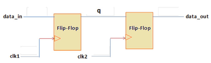
Figure 1 Multi-Clock Domain Concept
The timing is shown in Figure 2.
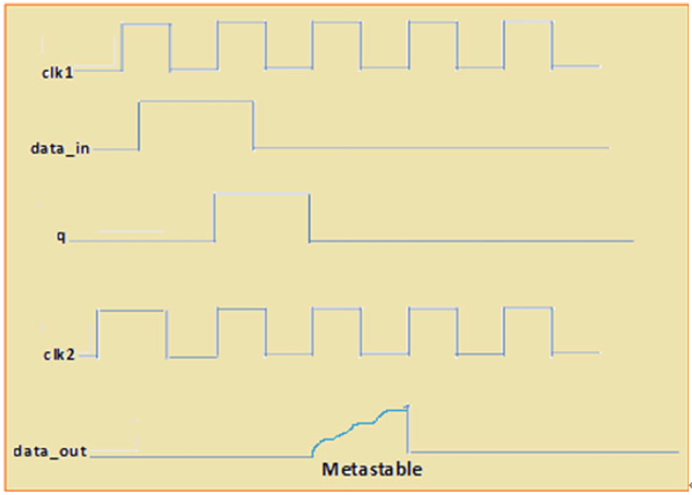
Figure 2 Metastable Output
03
Architectural Design Strategies
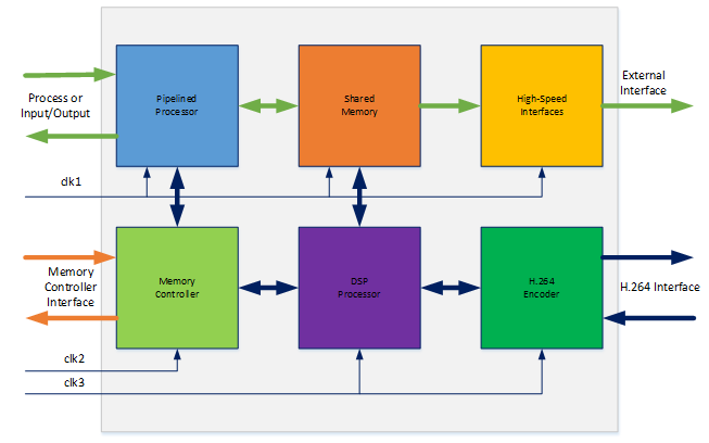
Figure 3 Multi-Clock Domain Architecture
Table 1 Multi-Clock Domain Clock Groups
|
Clock domain control |
Frequency in MHz |
Description |
|
clk1 |
500 |
The clock domain one operating at frequency of 500 MHz |
|
Clk2 |
666.66 |
The clock domain one operating at frequency of 666.66 MHz |
|
Clk3 |
250 |
The clock domain one operating at frequency of 250 MHz |
As an IC designer or architect, we need to consider the overall data integrity checks for multi-clock domain designs and provide clean timing for data and control paths.
With this in mind, we need to design synchronizers to transfer data between multi-clock domain designs. When transmitting control signals between multiple clock domains, synchronizers such as levels, multiplexers, and pulses are useful. Asynchronous FIFOs can be used as synchronizers to transfer data between clock domains and data paths.
Here are some guidelines to follow when performing multi-clock domain design to eliminate CDC errors.
Avoid Metastability:When passing control signal information, use register outputs, as this helps avoid glitches and hazards. By using registered output logic when passing control signals, multiple transitions within a single clock cycle can be avoided. The metastability blocking logic is shown in Figure 4.
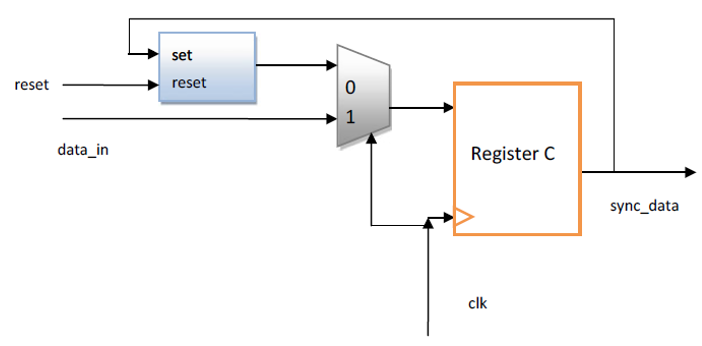
Figure 4 Metastability Blocking Logic
Use MCP:It is strongly recommended to use multi-cycle path strategies to avoid metastability issues when passing data and control signal information between multiple clock domains. In MCP, the strategy adopted is to establish control and data pairs, passing multi-bit data from the sending clock domain to the receiving clock domain with a single-bit control signal. Using pulse synchronizers can sample control information in the receiving clock domain and transfer data to the receiving clock domain with or without synchronizers. This technique can maintain a stable value of data over multiple cycles and can utilize the synchronizing signal generated by pulse synchronizers for sampling in the receiving clock domain. The following are key points to consider when crossing clock domain boundaries.
(a) Control signals must be synchronized using multi-stage synchronizers.
(b) Control signals should be free of hazards and glitches.
(c) There should be transitions across clock boundaries.
(d) Control signals should remain stable for at least one clock cycle.
The MCP strategy is illustrated in Figure 5.
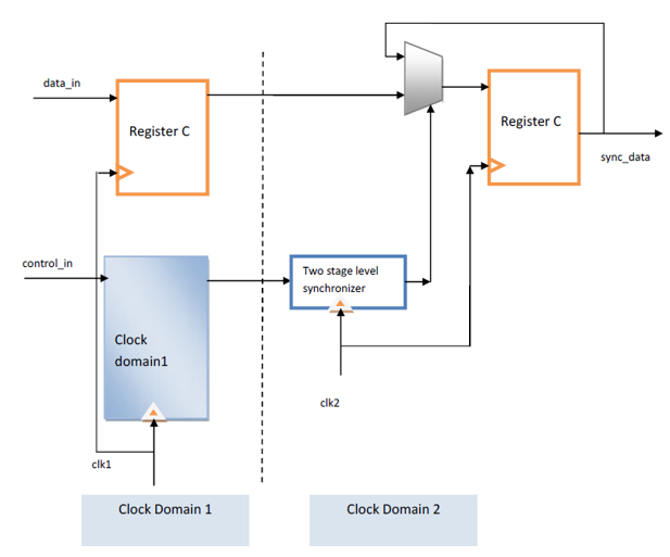
Figure 5 MCP Strategy
Use FIFO:Asynchronous FIFOs are an effective technique for passing multi-bit control signals or data information. In this technique, the sending clock domain writes data into the FIFO memory buffer when it is not full, and the receiving clock domain reads data from the FIFO buffer when it is not empty.
Use Gray Code Counter:In most ASIC designs with cross-clock domains (CDC), passing counter values across clock domain boundaries is crucial. If a binary counter is used to exchange data at the clock domain boundary, data transitions can easily go wrong due to one or more bit transitions. In this case, it is recommended to use a Gray code counter to pass data across clock boundaries. In the receiving clock domain, a conversion from Gray code to binary code is used to recover the original data.
Design Partitioning:When designing logic for multiple clock domains, partition the design using clock groups.
Clock Naming Conventions:To better identify clock sources, it is recommended to use clock naming conventions. The naming convention for clocks should be supported by meaningful prefixes/suffixes. For example, the sending clock domain uses clk_s, and the receiving clock domain uses clk_r.
Synchronize Reset:For ASIC designs, it is strongly recommended to use synchronous resetters.
Avoid Hold Time Violations:To avoid hold time violations, it is advisable to carefully review the architecture and develop strategies for passing stable data over multiple clock cycles.
Avoid Loss of Correlation:At clock domain boundaries, there are several possible ways to lose correlation. For instance:
(a) Multiple bits on the bus
(b) Multiple handshake signals
(c) Unrelated signals
To avoid this, use clock intent validation techniques, as these techniques will ensure the transmission of multi-bit signals across clock boundaries.
04
Control Path and Synchronization
This section discusses various synchronizers and strategies used in ASIC design.
Level or Multi-Trigger Synchronizers
Control signals transmitted between multiple clock domains are primarily passed from the fast clock domain to the slow clock domain, leading to timing errors and timing violations in the design. Therefore, during architectural design, a better strategy is to determine the interface boundaries of the multi-clock domain design and then use synchronizer strategies in the RTL design.
When passing control signals between multiple clock domains, metastability issues can be resolved by designing level synchronizers (possibly using two or three flip-flops). Figure 6 uses two-level level synchronizer logic.

Figure 6 Two-Level Level Synchronizer in Control Path
As shown in Figure 6, the level synchronizer transmits the control signal q1 from clock domain 1 to clock domain 2. The main design strategy is to pass the valid output q1 to the second clock domain. The level synchronizer samples the output q1 in the second clock domain. Due to setup or hold time violations, the input flip-flop in the second clock domain will be metastable, which should be ignored by setting EDA tool properties. The output data_out is valid data, and due to the use of the synchronizer, this design has a two-clock delay.
The timing description of the design shown in Figure 6 is as follows (shown in Figure 7).
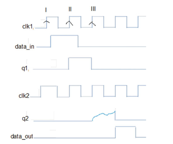
Figure 7 Timing with Two-Level Synchronizer
As shown in Figure 7, q1 is output by the first clock domain. On the rising edge of clk2, the output q2 of flip-flop FF1 will enter a metastable state due to setup or hold time violations. However, the output of flip-flop FF2 at the next clock edge is data_out, which is the valid output. The following command sets a false path:
set_false_path –from FF0/q –to FF1/qThe level synchronizer using these two flip-flops is shown in Figure 8, which can be adopted in the design. A better strategy is to treat the RTL description of the level synchronizer as a separate module during RTL design. The introduced delay depends on the number of flip-flops required to drive the output to a valid legal state.
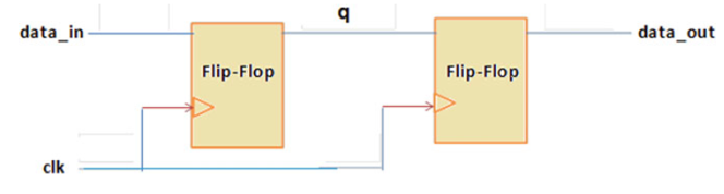
Figure 8 Level Synchronizer
Next, we will describe the RTL description part:
always @ (posedge clk)beginq&<=data_in;data_out&<=qendIn ASIC design, when control information needs to be passed from a fast clock domain to a slow clock domain, data integrity issues arise. This issue is caused by the non-convergence of the legal state of the flip-flop output when passing control signals from clock domain 1 to clock domain 2.
Utilizing pulse wideners can solve the sampling problem from the fast clock domain to the slow clock domain. Level pulse generators working on the positive clock edge are shown in Figure 9.
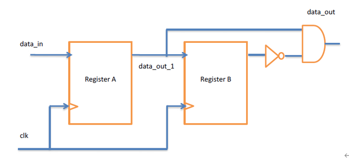
Figure 9 Level to Pulse Conversion
Another mechanism is the handshake of signals, which can be used to achieve data convergence.
As shown in Figure 10, the sampling signal of clock domain 2 is fed back to clock domain 1 as a handshake signal. This handshake mechanism serves as a confirmation or notification to the faster clock domain that the control signal passed from the faster clock domain has been successfully sampled by the slower clock domain. In most practical scenarios, this mechanism is employed, allowing the faster clock domain to send another control signal only after receiving a valid notification or acknowledgment signal from the slower clock domain.
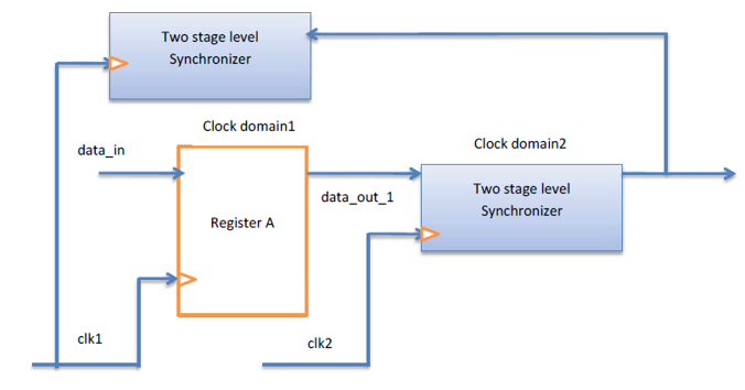
Figure 10 Handshake Mechanism for Control Signals
Pulse Synchronizer
This type of synchronizer uses multi-stage level synchronizers, where the output of the two-level level synchronizer is sampled by the output flip-flop. This synchronizer is also known as a toggle synchronizer, used to synchronize pulses generated from the sending clock domain to the target clock domain. When data is passed from the faster clock domain to the slower clock domain, if a two-level level synchronizer is used, pulses may skip. In this case, the pulse synchronizer is effective and useful. The pulse synchronizer diagram is shown in Figure 11.
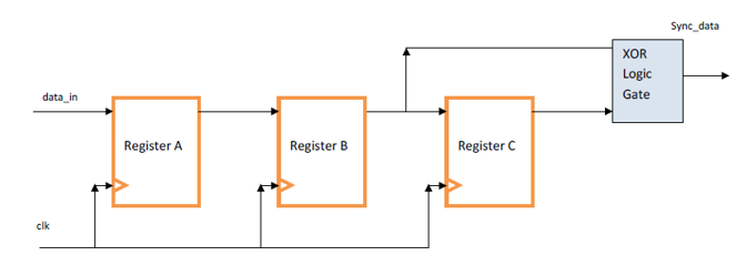
Figure 11 Pulse Synchronizer
Mux Synchronizer
When sending information from clock domain 1 to clock domain 2, this involves both data and control signals. Multi-bit data is used alongside a single-bit control signal. At the receiving end, based on the ratio of sending clock to receiving clock, control signals are generated for the multiplexer using level or pulse synchronizers. This technique is similar to MCP, and it is effective if the data is stable over multiple clock cycles when crossing clock boundaries. As shown in Figure 12.
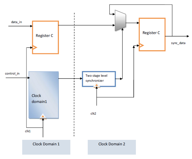
Figure 12 Mux Synchronizer
05
The Challenges of Multi-Bit Data Transmission
Passing multiple control signals between multiple clock domains is a significant challenge. The issue is that these control signals arrive at different times. If these control signals are not managed correctly, the real problem is due to skew. Consider the scenario shown in Figure 13, where “enable”, “load_en”, and “ready” need to be passed from one clock domain to another. In this case, if independent level synchronizers are used, the receiver may experience synchronization failures due to signal skew (different arrival times of signals).
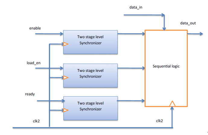
Figure 13 Sampling Multiple Signals in the Receiving Clock Domain
Consider one of the control signals, for example, if enable arrives later, there may be synchronization failures in the control path. To avoid this group of three control signals, try to pass common signals between clock domains. The strategy is illustrated in Figure 14.
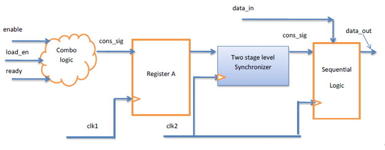
Figure 14 Control Signals Passed Fixed in Multi-Clock Domain
06
Data Path Synchronization
The techniques used to transmit multiple data bits across clock domains include:
-
Handshake Mechanism
-
Asynchronous FIFO Buffer
-
Gray Coding
Handshake Mechanism
The use of handshake mechanisms when passing multi-bit signals between clock domains is a useful technique. As shown in Figure 15, the transmitter operates at clk1, and the receiver operates at clk2. Data can be transmitted from the transmitter to the receiver. It is important to note that this handshake is slightly different from the handshake of the AXI bus.
The receiving clock domain can generate handshake signals such as data valid and device ready. Therefore, the goal is to notify the transmitter that there is still valid data available on the bus, and the device is not yet ready to receive new data.
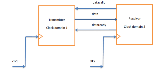
Figure 15 Handshake Mechanism Block Diagram
The handshake signal data valid is an active high handshake signal from clock domain 2, indicating that the transmitted data is valid data, and the receiver only needs a few clock cycles to sample that data. The clock delay during data transmission depends on the number of flip-flops used in the synchronizer, and the delay is one of the major drawbacks of the handshake mechanism.
The handshake signal device ready indicates that when the data is valid, the receiver is ready to receive new data, and the device is ready to pull high to notify the transmitter to put new data on the data bus.
If we have an FSM controller with multiple clock domains, then design the architecture to establish synchronization using request (request) and acknowledgment (ack) signals. The FSM controlled handshake mechanism is shown in Figure 16.
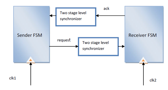
Figure 16 FSM Handshake Mechanism
Asynchronous FIFO Synchronizer
Asynchronous FIFOs are useful because data path synchronizers are used to exchange data between multiple clock domains. If the FIFO memory buffer is not full, the sending clock domain can write data into the FIFO memory buffer using write_clk, and if the FIFO memory buffer is not empty, the receiving clock domain can read data using read_clk (Figure 17).
FIFOs consist of several blocks:
Memory: Memory buffer
Write Clock Domain: Logic operating in the write clock domain on write_clk.
Read Clock Domain: Logic operating in the read clock domain on read_clk.
Flag Logic: Generates flag logic for empty and full.
FIFOs and related logic blocks are shown in Figure 17.
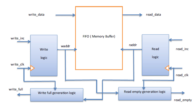
Figure 17 FIFO Block Diagram
How to determine the depth of FIFO?
Consider the write clock domain operating at 250 MHz, the read clock domain operating at 100 MHz, and no delay, then transmitting a burst length of 50 bytes can be calculated as follows:
Write clock time: T1 = 1/250 MHz = 4 ns. The Time Required to Write Burst of 50 Bytes of data = 4 ns*50 = 200 ns Read Clock Time: T2 = 1/100 MHz = 10 ns Number of Reads with 10 ns = 200 ns/10 ns = 20 Depth of FIFO = 50–20 = 30 Bytes.If read and write delays are specified, then try to modify the above steps to obtain the depth of FIFO.
Gray Coding
When passing multiple bits of data or control signals, it is necessary to use Gray coding techniques, as this technique ensures that only one bit changes between two consecutive numbers. For example, if 4-bit binary data needs to be passed between multiple clock domains, then one or more bits may change, requiring more power and increasing the chances of errors. Therefore, to avoid this and enhance performance, binary to Gray code conversion logic is used at the sending or transmitting clock domain. This ensures that only one bit changes at the clock boundary. To recover the original binary data in the receiving clock domain, Gray code to binary code conversion is used. This technique is illustrated in Figure 18.
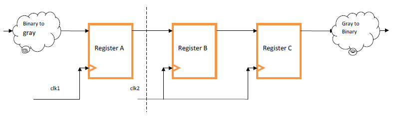
Figure 18 Gray Coding Technique
07
Conclusion
Summarizing a few key points:
-
When passing data between multiple clock domains, design data path synchronizers.
-
When passing control signals between multiple clock domains, it is necessary to design control path synchronizers.
-
It is strongly recommended to use multi-cycle paths to avoid metastability issues when passing data and control signal information across clock domains.
-
Common and effective techniques for passing multi-bit control or data information are the use of asynchronous FIFOs.
-
For multi-bit control signals transmitted across multiple clock domains, adopt grouping techniques to avoid skew caused by different arrival times.


E课网(www.eecourse.com) is a professional integrated circuit education platform under Moore Elite, dedicated to the cultivation of high-quality integrated circuit professionals in the semiconductor industry. The platform is oriented towards the job demands of integrated circuit companies, providing a practical training platform that fits the corporate environment, rapidly training students to meet corporate needs.
E课网 has a mature training platform, a complete curriculum system, and a strong teaching faculty, planning a high-quality semiconductor course system of 168 courses covering the entire integrated circuit industry chain, and has 4 offline training bases. To date, it has deeply trained a total of 15,367 people, directly supplying 4,476 professional talents to the industry. It has established deep cooperative relationships with 143 universities and has held 240 corporate special IC training sessions.