For a wealth of sensor knowledge and industry reports, please reply with the keyword 【资料下载】 in the public account dialog to obtain materials for viewing.《Over 100 Professional Knowledge Materials on Sensors, There’s Always One for You~》
Follow me here 👇,Remember to click the menu bar in the top right corner ••• Set as Star ⭐
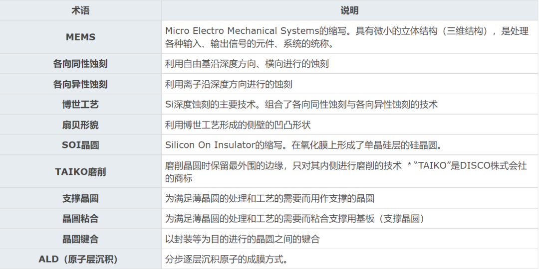
MEMS technology has profoundly influenced the development of modern sensors, serving as the key technology for sensor miniaturization, low power consumption, and intelligence. MEMS sensors manufactured using MEMS technology occupy an important share among various sensors.
Among them, MEMS chips and ASIC chips are the parts with the highest technology and value content in a MEMS sensor.Do you know how MEMS chips are manufactured? What is the difference between MEMS chips and integrated circuit chips?
What are the main structures of MEMS sensors? What is the difference between MEMS chips and integrated circuit chips?
MEMS stands for Micro-Electro-Mechanical System, which is an industrial technology that integrates microelectronic circuit technology with micro-mechanical systems, operating at a micrometer scale.
Furthermore, there is also a Nano-Electro-Mechanical System (NEMS), a type of device that integrates electrical and mechanical functions at a smaller nanoscale. NEMS technology still faces some challenges in mass production and commercialization.
The new sensors manufactured using MEMS technology are called MEMS sensors. Generally, the main structure of a sensor consists of four parts: the sensitive element, the conversion element, the transformation circuit, and the auxiliary power supply. So, what is the main structure of a MEMS sensor?
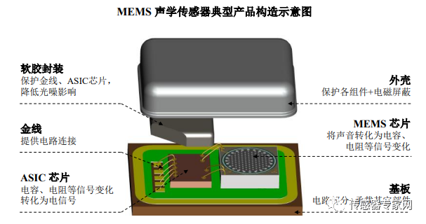
The following is a typical product structure schematic of a MEMS acoustic sensor. We can see that the structure of the MEMS sensor mainly consists of the MEMS chip — used to sense signals, equivalent to the sensitive element; and the ASIC chip — used to process signals, equivalent to the conversion and transformation elements.
MEMS chips and ASIC chips are also the parts with the highest technology and value content in a MEMS sensor. For the principles and structures of common MEMS sensors, please refer to 《10 Major MEMS Sensor Principles Fully Explained!》, which will not be elaborated on in this article.
▲Structure diagram of a MEMS acoustic sensor (from GoerTek’s prospectus)
So, what is the difference between MEMS chips and integrated circuit chips?
The manufacturing technology of MEMS devices mainly includes integrated circuit technology represented by the United States, MEMS technology characterized by precision processing in Japan, and LIGA technology in Germany. Currently, MEMS chips use integrated circuit technology, which is also the most widely used method for manufacturing MEMS devices.
Similar to integrated circuits, MEMS chips widely use silicon as the wafer substrate material. The individual processes used in integrated circuit manufacturing, such as photolithography, thin film deposition, etching, and doping, have also become the universal techniques for MEMS chip manufacturing, mainly divided into: front-end processes and back-end packaging processes. Among them, the front-end processes mainly include wafer cleaning, photolithography, etching, etc.; the back-end packaging processes mainly include testing, packaging, and finished product inspection.
Although MEMS chips and integrated circuit chips are both micro-components on semiconductor wafers, there are still some differences between the two. Compared to integrated circuit chips, MEMS chips control physical phenomena through micro-mechanical structures and convert them into electrical signals, enabling interaction between mechanical and electronic components. Integrated circuit chips mainly transmit signals using current, electromagnetism, and other methods.
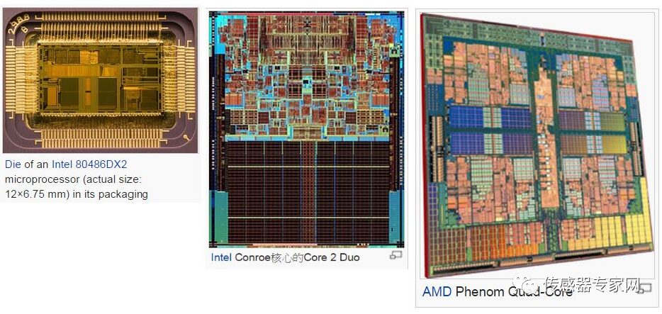
Ordinary integrated circuit chips interconnect the transistors, resistors, capacitors, and inductors required in a circuit within the semiconductor crystal to pack more transistors and components into a given area of the wafer (which represents stronger performance). Thus, integrated circuit chips pursue higher process technology, such as CPUs, GPUs, and other logic chips, as well as memory chips.
▲The internal structure of an integrated circuit CPU chip with densely packed transistors and other components
Compared to integrated circuit chips, MEMS chips contain mechanical structures, enabling interaction between mechanical and electronic components. Additionally, micro-electromechanical systems consist of components sized from 1 to 100 micrometers, where typical sizes of micro-electromechanical devices range from 20 micrometers to one millimeter. Unlike integrated circuit chips, which do not need to pursue advanced process technology, MEMS chips focus more on the development of manufacturing processes.
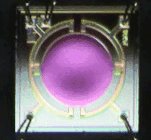
▲Mechanical structure and movement of a MEMS microphone chip (captured by a high-precision image sensor)
▲The structure of a MEMS accelerometer chip
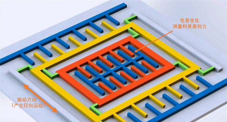
▲The internal structure of a MEMS gyroscope chip
The above shows the internal structures of the MEMS microphone chip, MEMS accelerometer chip, and MEMS gyroscope chip, visually demonstrating their different mechanical structural features (for related principles and structures, please refer to 《10 Major MEMS Sensor Principles Fully Explained!》).
At the same time, the mechanical structural characteristics of each MEMS sensor chip are quite different, which is why there is a saying that “one product, one process” for MEMS chips. Currently, there is no unified process that can meet the manufacturing needs of all MEMS devices, which also limits the mass production and R&D speed of MEMS sensors. Therefore, general MEMS processes have become one of the key research focuses in MEMS sensor chips.
What is an ASIC chip? What makes the ASIC chip of a MEMS sensor special compared to other ASIC chips?
As mentioned above, the most important chips in a MEMS sensor are the MEMS chip and the ASIC chip, where the MEMS chip is responsible for sensing signals and converting the measurement into changes in resistance, capacitance, etc.; the ASIC chip is responsible for converting capacitance, resistance, and other signals into electrical signals, involving functions such as signal conversion and amplification.
ASIC stands for Application-specific Integrated Circuit, referring to dedicated chips developed for specific functions. The ASIC chip in a MEMS sensor uses the same manufacturing process as integrated circuit chips, as it does not contain mechanical structures.
However, due to the uniqueness of MEMS chips, their analog output is often very weak or has unconventional usage conditions, and general ASIC chips cannot meet their requirements. Conventional ASIC design companies also cannot design chips that satisfy MEMS sensor manufacturers. This has led to the widespread phenomenon of “chip shortages” in the MEMS industry, where “chip” refers to ASICs specifically for MEMS. Therefore, the design of MEMS-specific ASICs is a key common technology in the development of MEMS technology.
Previously, the European Union adopted a “national system,” gathering 10 companies from 7 countries to spend 140 million yuan to develop the next generation of high-efficiency readout integrated circuit chips for infrared sensors, which belongs to the research and development of sensor ASIC chips. (See 《EU Develops Infrared Sensors with National System》)
The Main Manufacturing Processes of MEMS Chips
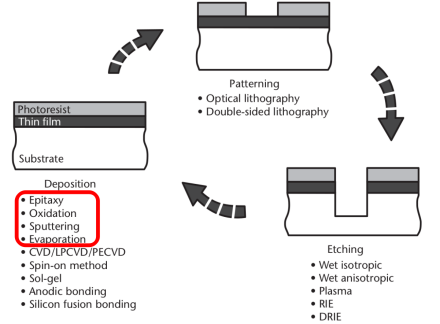
The manufacturing of MEMS chips involves basic process steps such asphotolithography, dry etching, wet etching, thin film deposition, oxidation, diffusion, injection, sputtering, vapor deposition, bonding, etc., to create complex three-dimensional micro-machining technology. With years of development, the MEMS field has also seen some specialized processes, such asanisotropic wet etching, wafer bonding, deep reactive ion etching, etc., but their application is still limited to MEMS and has not yet been applied back to the IC industry.
Generally, the basic processes for MEMS chip manufacturing include three key steps: Deposition, Patterning, and Etching. The entire process is: ① Coating the wafer/substrate with photoresist, then ② Exposing the photoresist to remove the non-patterned portions of the photoresist, and then ③ Using the photoresist as a mask to etch the underlying material. This entire process is repeated until the microstructure is completed.
Figure – Basic Process Flow of MEMS Manufacturing
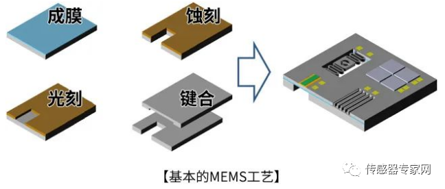
MEMS processes are based on conventional semiconductor process flows such as film forming, photolithography, etching, bonding, etc. In addition to general processes, due to the particularity of MEMS device structures, many special manufacturing processes have also emerged.
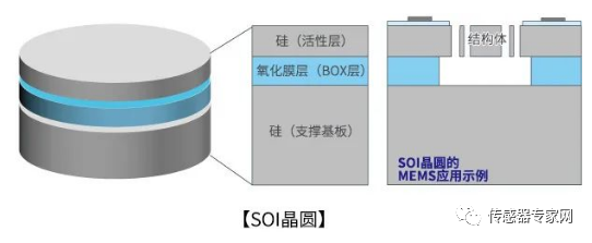
SOI stands for Silicon On Insulator, referring to silicon wafers with a single crystal silicon layer formed on an oxide film. It has been widely used in power devices and MEMS, etc., and in MEMS, the oxide film layer can be used as an etch stop layer for silicon, thus enabling the formation of complex three-dimensional structures.
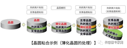
Wafer Bonding/Thermal Release Film Process
Using support wafers and thermal release films can easily process thinned wafers.
For the high integration of MEMS devices with CMOS chips, and since many MEMS are based on SOI wafers and other technology substrates, these demands heavily rely on the important process of wafer bonding.
Wafer bonding refers to the technology that enables two substrate materials (such as silicon-silicon or silicon-glass) to form sufficient contact under certain external conditions (temperature, pressure, voltage, etc.), ultimately bonding the two substrate materials into one through the molecular or chemical bond forces formed at the interface between adjacent materials. Currently, wafer bonding technology can be divided into two major categories: one that does not require a medium layer for bonding, such as Si-Si bonding; and another that requires a medium layer for bonding, such as polymer bonding.
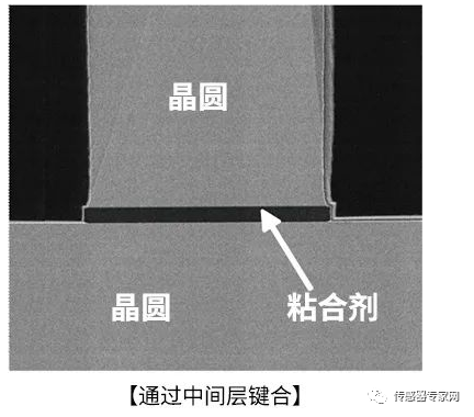
Wafer bonding is roughly divided into “Direct Bonding” and “Bonding via Intermediate Layer”.
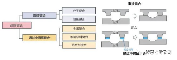
Direct bonding does not use adhesives and relies on intermolecular forces generated by heat treatment to bond the wafers, used for making SOI wafers, etc.
Bonding via an intermediate layer uses adhesives to bond the wafers together.
Three Manufacturing Processes of MEMS Chips
MEMS manufacturing processes mainly include surface micromachining, bulk micromachining, and LIGA technology, with the first two being the most widely applied and technically mature.
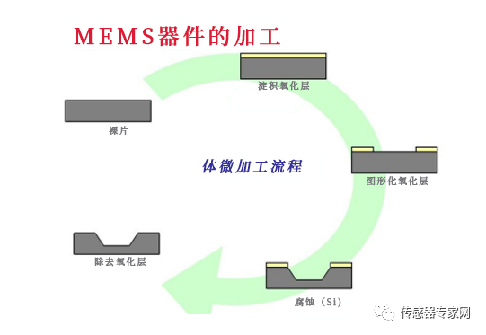
Bulk Micromachining refers to the process of etching the silicon substrate from top to bottom, which is a technique for manufacturing various mechanical structure devices on the silicon substrate through anisotropic or isotropic etching methods, including wet etching and dry etching, and is an important method for preparing MEMS devices with three-dimensional structures. Its characteristics include simple equipment and low investment, but it can only produce simple-shaped devices with a low aspect ratio. It is obtained by etching silicon material, consuming a lot of silicon material (sometimes referred to as subtractive processing), and can only process silicon material.
▲Bulk micromachining process of MEMS chips
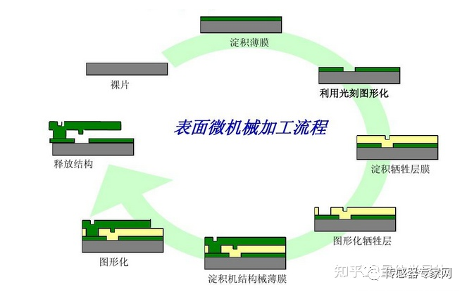
Surface Micromachining utilizes thin film deposition, photolithography, and etching methods to add materials layer by layer on the substrate, using surface growth methods and photolithography to manufacture various micro-mechanical structure devices on the surface, and finally removing the sacrificial layer to construct microstructures. Various materials such as metals, polysilicon, nitrides, oxides, and organic materials are deposited and etched on the top surface of the substrate.
Common deposition techniques include vapor deposition, sputtering, screen printing, CVD (Chemical Vapor Deposition), and electroplating, etc. It also employs dry etching and wet etching techniques. Its characteristics allow for the creation of more complex parts by adding various materials to silicon, but the technology is more complex and the equipment is relatively expensive.
▲Surface micromachining process of MEMS chips
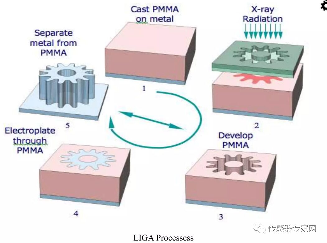
LIGA Process (Lithography, Electroforming, and Molding) is an abbreviation for the German terms Lithographie (lithography), Galvanoformung (electroforming), and Abformung (molding). The LIGA technology can process non-silicon materials such as metals and plastics, and can also process parts with a large aspect ratio, which is difficult for bulk micromachining and surface micromachining. However, this process requires high-energy rays produced by synchrotron radiation devices as the primary processing method, making the equipment expensive and requiring significant investment.
The LIGA process consists of four components: LIGA mask manufacturing process; X-ray deep lithography process; micro-electroforming process; and micro-replication process.
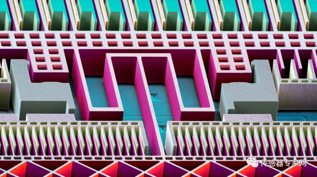
The main material used in MEMS is silicon, as the most fundamental technology in MEMS processing is the etching technology of silicon. Using the anisotropic etching of silicon allows for different etching rates based on the crystalline orientation of silicon, forming specific mechanical structures. Silicon has excellent mechanical properties, meeting the mechanical characteristics required for most micro-sensors and micro-actuators, and using silicon allows for integration with ICs, forming more complex microsystems.
▲Mechanical structures formed in MEMS sensor chips after etching
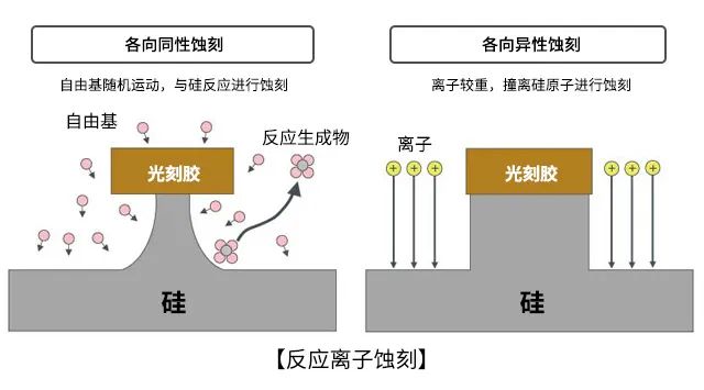
Isotropic Etching vs. Anisotropic Etching
Reactive ion etching is a technique that generates ions and other particles by discharging in a low vacuum to perform etching using these particles.
In the plasma, there are charged ions and neutral free radicals, enabling both isotropic etching using free radicals and anisotropic etching using ions.
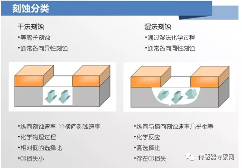
Wet Etching and Dry Deep Etching in MEMS Chips
The wet anisotropic etching of silicon is the earliest developed micro-machining technology. Wet etching utilizes a chemical reaction between the material being etched and the etching solution, while dry deep etching employs deep reactive ion etching (DRIE) for anisotropic etching of silicon, which is a newly developed deep etching technology since the 1970s.
Wet etching requires etching solutions, reactors, temperature control devices, cleaning machines, etc. Common anisotropic etching solutions include KOH solution and ammonium hydroxide (TMAH) aqueous solution. The etching rate of these alkaline solutions on silicon is related to the crystal phase. Due to its simple process and lower cost, wet etching is widely used in devices such as accelerometers and pressure sensors.
Dry deep etching uses fluorinated gas hexafluoride (SF6) plasma for etching, while protective gases convert isotropic etching of SF6 into anisotropic etching, enabling deep etching. DRIE is mainly divided into Bosch process and low-temperature etching process.Dry deep etching technology offers a larger processing space compared to wet etching.
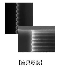
The Bosch process, which combines the advantages of both anisotropic and isotropic etching, has become the mainstream technology for silicon deep etching.
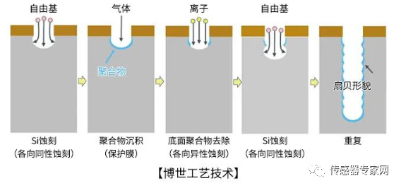
By repeatedly performing Si etching ⇒ polymer deposition ⇒ removal of bottom polymer, longitudinal deep etching can be achieved.
The unevenness of the sidewalls resembles a scallop, referred to as “scalloped morphology.”
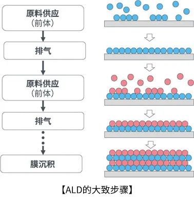
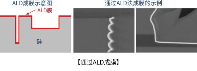
ALD (Atomic Layer Deposition) ALD stands for Atomic Layer Deposition, which is a method of stepwise layer-by-layer deposition of atoms through repeated material supply (precursors) and exhaust, using surface reactions between the precursors and the substrate.
By using this method, as long as there is a gap through which the film-forming material can pass, it is possible to control the film thickness at the nanoscale, forming films on the sidewalls of small holes and at the bottom of deep holes during MEMS processing.
The main material for MEMS devices is silicon, as the most fundamental technology in MEMS processing is the etching technology of silicon, which comes from the photolithography, thin film deposition, etching, and doping processes used in integrated circuit chip manufacturing, and is also the universal process for MEMS chips.
MEMS sensors are ubiquitous, from smartphones to automobiles, from smart factories to medical devices. According to relevant data, nearly three-quarters of semiconductor sensor sales come from products manufactured using MEMS technology.MEMS devices now account for 54% of the total global sensor shipments.
The semiconductor manufacturing processes required for MEMS chips are mainly at the micrometer level and do not involve advanced processes. Currently, advanced countries have not prohibited China from obtaining MEMS manufacturing equipment, and mainland China’s semiconductor equipment can meet local MEMS manufacturing needs.
The R&D of domestic MEMS sensors faces mainly issues of process improvement, market expansion, etc. With the increasing attention from local governments in recent years, the investment in MEMS pilot lines and mass production lines across various regions will help establish a common basic process production system for MEMS, enhance the R&D and iteration capabilities of sensor companies in MEMS processes, and promote the rapid development of China’s MEMS sensor industry.
MEMS is expected to become a breakthrough point for China’s semiconductor industry!
Some of the materials in this article are sourced from:
Shanghai Institute of Microsystem and Information Technology “Introduction to the 8-inch Line Bonding Process” and other contents
What is MEMS? A 4-step diagram of MEMS chip manufacturing
Hu Yisen from the School of Mechanical Engineering, Nanjing University of Science and Technology “Overview of Micro-Electromechanical System Manufacturing Processes”
What do you think of this article? Feel free to leave your comments below the content on the Sensor Expert Network public account, or engage in discussions in China’s largest sensor community: Sensor Exchange Circle.
What do you think of this article? Feel free to leave a message and share!
Share and click to see, and let more people understand the dynamics of China’s sensor industry!
The starred content = the content you care about. According to the recommendation principles of WeChat public accounts, if you do not set the Sensor Expert Network public account homepage as a star, you will not be able to receive the latest information in the sensor industry in a timely manner!
Disclaimer: The content of this article is the author’s personal opinion and does not represent the views or positions of the Sensor Expert Network. If there is any infringement or other matters, please contact via WeChat: MM380702. For more opinions, everyone is welcome to leave comments.
-
Finally understood, modern warfare is all about sensors
-
The richest chipmaker in China actually comes from sensors
-
Woke up one day and found that Chinese companies can no longer design sensors?!