Welcome FPGA engineers to join the official WeChat technical group
Clickthe blue textto follow us at FPGA Home – the best and largest pure FPGA engineer community in China

1
Introduction to FPGA
FPGA has a wider range of applications than we usually imagine, due to the greater variety of integrated modules, not just the original simple logic elements (LE).
Today’s FPGAs not only include the previous LEs, but also have larger, faster, and more flexible RAM, more complex IOBs, and support for more I/O types, while also integrating some special functional units, including the following:
DSP: Essentially a multiplier-accumulator, multiple multipliers can be integrated within an FPGA, while a typical DSP chip often has only one core. In other words, FPGAs can more easily implement multiple DSP core functions. In scenarios requiring a large number of multiply-accumulate calculations, the speed of multiple multipliers working in parallel can far exceed that of a single high-speed multiplier.
SERDES: High-speed serial interfaces. In the future, PCI-E, XAUI, HT, S-ATA, and other high-speed serial interfaces will become more prevalent. With the SERDES module, FPGAs can easily integrate these high-speed serial interfaces without needing to purchase dedicated interface chips.
CPU core: Divided into two types, soft core and hard core. Soft cores are CPU modules written in logic code that can be implemented in any FPGA with sufficient resources, offering great flexibility. Additionally, multiple soft cores can be integrated in large-capacity FPGAs for multi-core parallel processing. Hard cores are CPU cores pre-implemented within specific FPGAs, with the advantage of speed and performance but lacking flexibility.
However, FPGAs still have drawbacks. For certain high-frequency applications, FPGAs may fall short. Although theoretically, FPGAs can support 500MHz, in practical designs, achieving a working frequency above 200MHz is often quite challenging. Now, let’s get to the main topic: the key points of FPGA design.
2
History of FPGA Development
The history of FPGA development is shown in the following diagram. Compared to PROM, PAL/GAL, and CPLD, FPGAs have larger scales and higher performance.
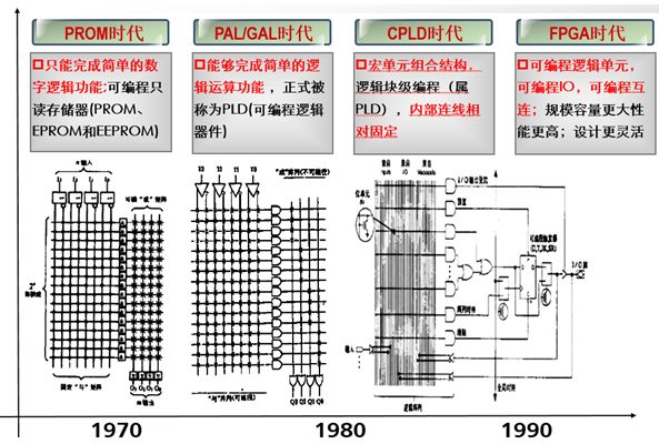
Figure 1: History of FPGA Development
The mainstream FPGA chip manufacturers include Xilinx, Altera, Lattice, and Microsemi, with the first two accounting for a combined market share of 88%. Currently, all mainstream FPGA manufacturers are based in the United States. Domestic FPGAs, having started R&D at least 20 years later than the US, are still in a growth phase and are limited to low-end applications, with no mature applications in the communication market.
In December 2015, Intel acquired Altera for $16.7 billion. Shortly after the acquisition, Altera established a product roadmap for integrating Intel processors with FPGAs. The benefit of integrating these two products is that it can provide innovative heterogeneous multi-core architectures to meet the demands of new markets such as artificial intelligence, while significantly reducing power consumption.

Figure 2: Application History of FPGA in Telecommunications
FPGAs have very mature and widespread applications in aerospace, military, and telecommunications fields. For example, in the telecommunications equipment integration phase, FPGAs are used for network protocol analysis and interface conversion due to their programming flexibility and high performance.
-
In the NFV (Network Function Virtualization) phase, FPGAs achieve a 5-fold performance improvement for network element data planes based on general servers and hypervisors, while also being manageable and orchestrated by the general OpenStack framework.
-
In the cloud era, FPGAs have been used as basic IaaS resources to provide development and acceleration services in public clouds, with AWS, Huawei, and BAT all offering similar general services.
-
As of now, Intel’s Stratix 10 devices have been successfully applied in Microsoft’s real-time AI cloud platform, Brainwave.
3
Overall Structure of FPGA
The architecture of FPGA mainly includes four parts: Configurable Logic Blocks (CLB), Input Output Blocks (IOB), internal interconnects, and other embedded units.
CLB is the basic logic unit of FPGA. The actual number and characteristics may vary depending on the device, but each CLB contains a configurable switch matrix made up of 4 or 6 inputs, several selection circuits (multiplexers, etc.), and flip-flops. The switch matrix has a high degree of flexibility and can be configured to handle combinational logic, shift registers, or RAM.
FPGAs can support many I/O standards, thus providing ideal interface bridging for system design. The I/O within an FPGA is grouped by banks, and each bank can independently support different I/O standards. The most advanced FPGAs currently offer over ten I/O banks, providing flexible I/O support.
CLB provides logical performance, while flexible interconnect routing is responsible for transmitting signals between CLB and I/O. There are several types of routing, from those designed specifically for CLB interconnections (short-line resources), to high-speed horizontal and vertical long lines within the device (long-line resources), and global low-skew routing for clocks and other global signals (global dedicated routing resources). Generally, design software from manufacturers hides the interconnect routing tasks from the user, significantly reducing design complexity.
Embedded hard core units include RAM, DSP, DCM (Digital Clock Management Module), and other specific interface hard cores. The internal structure of FPGA devices is shown in the following diagram.
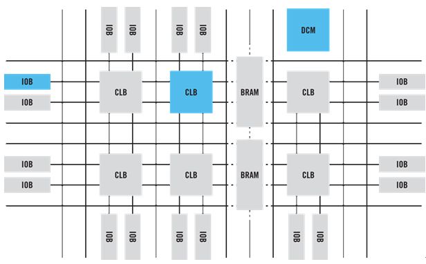
Figure 3: Internal Structure Diagram of FPGA Devices
Generally speaking, the larger the device model number, the larger the logical resource scale the device can provide. When selecting FPGA devices, users need to refer to this table and comprehensively consider the project’s most suitable logic device based on various needs such as logical resources (CLB), internal BlockRAM, interfaces (number of high-speed Serdes), digital signal processing (number of DSP hard cores), and future expansion.
4
FPGA Development Process
The FPGA design process involves using EDA development software and programming tools to develop FPGA chips. The general FPGA development process is shown in the following diagram, including main steps such as function definition/device selection, design input, functional simulation, logic synthesis, layout and routing, and programming/debugging.
1. Function definition/device selection: Before starting an FPGA design project, a definition of system functionality and module division must be established. Additionally, based on task requirements, such as system functionality and complexity, trade-offs must be made regarding operational speed, device resources, costs, and routability to select appropriate design schemes and device types.
2. Design input: Design input refers to using hardware description languages to express the designed system or circuit in code. The most commonly used hardware description language is Verilog HDL.
3. Functional simulation: Functional simulation refers to logically verifying the user’s designed circuit before logic synthesis. Before simulation, a test platform must be set up, and test stimuli prepared. The simulation results will generate report files and output signal waveforms, from which the changes in signals at various nodes can be observed. If errors are found, the design must be returned for modification. Common simulation tools include Model Tech’s ModelSim and Synopsys’s VCS.
4. Logic synthesis: Synthesis refers to transforming higher-level abstract descriptions into lower-level descriptions. Synthesis optimization optimizes the generated logic connections based on goals and requirements, flattening hierarchical designs for implementation by FPGA layout and routing software. At the current level, synthesis optimization refers to compiling design inputs into a logic connection netlist consisting of basic logic units such as AND gates, OR gates, NOT gates, RAM, and flip-flops, rather than a real gate-level circuit.
A real specific gate-level circuit must be generated using the layout and routing features of FPGA manufacturers, based on the standard gate-level structure netlist generated after synthesis. To convert into a standard gate-level structure netlist, the HDL program must be written according to the style required by specific synthesizers. Common synthesis tools include Synplicity’s Synplify/Synplify Pro software and various synthesis development tools released by FPGA manufacturers themselves.
5. Layout and routing: Layout and routing can be understood as using implementation tools to map logic into the resources of the target device structure, determining the optimal layout for logic, selecting routing channels for linking logic and input/output functions, and generating corresponding files (such as configuration files and related reports); implementation configures the logic netlist generated by synthesis onto specific FPGA chips. Since only FPGA chip manufacturers have the best understanding of chip structures, layout and routing must use tools provided by chip developers.
6. Programming/debugging: The final step of design is programming and debugging. Chip programming refers to generating the data files (bitstream generation) needed for use, loading the programming data into the FPGA chip; then, board testing can be conducted. Finally, the FPGA file (such as .bit file) is downloaded from the computer to the FPGA chip on the single board.
5
How to Use FPGA
Once FPGA development is complete, the validated loading file is obtained. After outputting the loading file, normal business processing and verification can begin (for example, describing the entire process in a software loading manner)
-
1. Logic loading;
-
2. After loading the logic onto the single board software, a logic reset is required;
-
3. After the reset is complete, the software must wait for a period until the logic Phase-Locked Loop (PLL) stabilizes;
-
4. The software initiates self-check operations for external RAM, internal Block RAM, DDRC, etc.;
-
5. After self-checking, the software initializes all writable RAM spaces and registers;
-
6. After initialization, the software configures register items and settings according to the logic chip manual;
-
7. Once the logic is ready, business processing can begin.
6
Applicable Scenarios for FPGA
FPGAs are suitable for irregular, highly concurrent, intensive computation, and protocol parsing processing scenarios, such as artificial intelligence, gene sequencing, video encoding, data compression, image processing, network processing, and other fields of acceleration.
7
Key Point of FPGA Design 1: Clock Tree
For FPGAs, it is essential to avoid asynchronous designs as much as possible and adopt synchronous designs.
The first key to synchronous design, and the most critical, is the clock tree.
A poor clock tree is an irreparable disaster for FPGA design; it’s like a building built on a poor foundation, and its collapse is inevitable.
Some specific design details:
1) Use a single clock as much as possible;
2) If there are multiple clock domains, they must be carefully divided;
3) Signals crossing clock domains must be synchronized. For control signals, double sampling can be used; for data signals, asynchronous FIFO can be used. It should be noted that asynchronous FIFO is not a universal solution; it can only solve frequency difference issues within a certain range.
4) Utilize the PLL and DLL within the FPGA as much as possible, as this will bring significant benefits to your design.
5) For special I/O interfaces, carefully calculate Tsu, Tco, Th, and utilize various tools such as PLL, DLL, DDIO, and pin-configurable delays. Simply constraining Tsu, Tco, Th for pins is often insufficient.
It may not be very precise to say this. The clock tree here actually refers to the clock scheme, mainly the planning of clock domains and PLL, and generally does not involve detailed calculations of line delays (as they typically use global clock networks and local clock networks with fixed delays), which is different from ASIC. For ASICs, careful analysis and calculation of clock network design, routing, and delays are essential.
8
Key Point of FPGA Design 2: FSM
FSM: Finite State Machine. This can be considered the foundation of logic design. Almost every slightly larger logic design will have FSM.
FSM can be divided into Moore type and Mealy type; Moore type’s state transitions are independent of variables, while Mealy type’s are related. In practice, the majority used are Mealy type.
There are generally two ways to write FSM: single-process and dual-process.
Beginners often prefer the single-process writing style, formatted as follows:

In simple terms, a single-process FSM is where all synchronous and asynchronous processing is placed within a single always block.
Advantages:
1) It appears relatively simple and clear, and you don’t have to write the handling of each signal and state signal in every case or if branch. You can also simply add some counters for counting.
2) All output signals are already latched by D flip-flops.
Disadvantages:
1) The optimization effect is poor. Since synchronous and asynchronous are mixed together, the compiler generally optimizes asynchronous logic best. The result of mixing synchronous and asynchronous in a single-process FSM leads to poor optimization effects, often resulting in slower logic speed and higher resource consumption.
2) Sometimes faster signal outputs are needed without going through D flip-flops, which makes processing in a single-process FSM more complicated.
The dual-process FSM is formatted as follows:
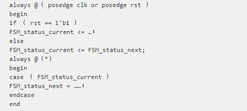
As seen above, synchronous and asynchronous processes are placed in two separate always blocks. The FSM state variables also use two to control. I won’t go into the details of the dual-process FSM principle here, as it is covered in many logic design books; everyone can take a look.
Advantages:
1) The compiler’s optimization effect is significant, achieving very favorable speed and resource utilization rates.
2) All output signals (except FSM_status_current) are combinational outputs, making them faster than single-process FSM.
Disadvantages:
1) All output signals (except FSM_status_current) are combinational outputs, and in some cases, extra code needs to be written for latching.
2) In the asynchronous processing always block, all if and case branches must assign all output signals, and signals from the FSM must not be assigned back to other signals in the FSM, or it will lead to latches.
Latches can lead to the following issues:
1) Functional simulation results do not match post-simulation;
2) Logic that cannot be tested appears;
3) Logic becomes unstable, especially latches are sensitive to glitches;
4) In some very special cases, if positive feedback occurs, it may lead to disastrous consequences.
This is not a scare tactic or a joke; I have seen a guy load his logic onto the FPGA, and the entire FPGA blew up. Later, it was suspected that positive feedback caused high-frequency oscillation, ultimately leading to the chip overheating and exploding (this FPGA chip did not have a heat sink installed).
9
Key Point of FPGA Design 3: Latch
First, let me explain:
1) I haven’t used stateCAD, but I feel that using this tool for building large systems seems inconvenient. Perhaps using SystemC or SystemVerilog would be better.
2) The terms synchronous and asynchronous are habits at my company and may not be entirely accurate, but I am used to them, haha.
Now, let’s talk about latches:
I previously discussed the dangers of latches; now let’s talk about how to avoid them. I have summarized the following points:
1) In combinational logic processes, if statements must have an else! And all signals must be assigned in all branches of the if.
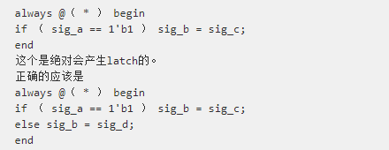
Additionally, it is important to note that the following can also generate latches. This means that in combinational logic processes, you cannot have situations where a signal assigns itself or indirectly assigns itself.

However, this issue does not exist in sequential logic processes.
2) The default case in case statements must not be omitted! The reason is the same as for if statements, and I won’t elaborate further.
It should be noted that in sequential logic processes, the default statement must also be included; this is a good habit.
3) The sensitive variables in combinational logic processes cannot be fewer or more. This issue is not too significant, as Verilog 2001 syntax can directly handle it with *.
In conclusion, latches have disadvantages but also advantages. In FPGA’s LE, there is always a latch and a D flip-flop, and in IOBs supporting DDR, there is also a latch to implement DDIO. However, in our regular designs, we should avoid latches as much as possible.
10
Key Point of FPGA Design 4: Logic Simulation
Simulation is an essential step in FPGA design. Without simulation, there is nothing.
Simulation is a monotonous and tedious task, making it easy to feel like giving up or cutting corners. At this time, you must hold on!
Simulation can be divided into unit simulation, integration simulation, and system simulation.
Unit simulation: Simulation for each minimum basic module. Unit simulation requires code line coverage, condition branch coverage, and expression coverage to reach 100%! These three coverage metrics can be checked through MODELSIM, but the compile option must be set correctly when compiling the module.
Integration simulation: Simulating multiple large modules together. Coverage requirements should be as high as possible.
System simulation: Simulating the entire hardware system together. At this point, the entire simulation platform includes simulation models for the logic peripheral chip interfaces, as well as BFM, Testbench, etc. System simulation requires carefully designing simulation test cases and simulation testing platforms based on the functional and performance requirements of the logic being simulated. System simulation is a significant branch of logic design and a discipline that requires specialized study.

Welcome communication engineers and FPGA engineers to follow our public account

Welcome to join the largest national FPGA WeChat technical group
This group has tens of thousands of engineers, a community of engineers passionate about technology, where FPGA engineers help each other and share knowledge, creating a strong technical atmosphere! Hurry up and invite your friends to join!!

Press and hold to join the FPGA national technical group
FPGA Home Component City
Advantageous component services, please scan to contact the group owner: Jin Juan Email: [email protected] Welcome to recommend to procurement
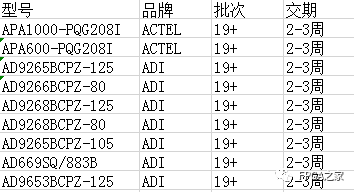
ACTEL, AD part of the advantageous ordering (operating the full series):
XILINX, ALTERA advantageous stock or ordering (operating the full series):
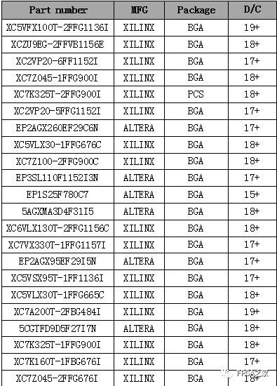
(The above components are part of the models; for more models, please consult the group owner Jin Juan)
Service philosophy: FPGA Home component self-operated city aims to facilitate engineers to quickly and conveniently purchase component services. After years of dedicated service, our customer service is spread across large domestic listed companies, military research units, small and medium enterprises, with the biggest advantage being emphasizing service first, and achieving quick delivery and favorable prices!
Directly operated brands: Xilinx ALTERA ADI TI NXP ST E2V, Micron and over a hundred component brands, especially skilled in components under US embargo against China. Engineers are welcome to recommend us to procurement or consult us personally! We will continue to provide the best service in the industry!

Official thanks to the FPGA technical group brands: Xilinx, Intel (Altera), Microsemi (Actel), Lattice, Vantis, Quicklogic, Lucent, etc.