Main reference materials:
Bilibili @ Jiangxie Technology
STM32 Beginner Tutorial – 2023 Edition Detailed Explanation with Chinese Subtitles
Development material download link: https://pan.baidu.com/s/1h_UjuQKDX9IpP-U1Effbsw?pwd=dspb
Microcontroller kit: STM32F103C8T6 development board microcontroller C6T6 core board experimental board minimum system board kit (available for purchase at the end of the article)
SPI Communication
- • SPI (Serial Peripheral Interface) is a general-purpose data bus developed by Motorola.
- • Four communication lines: SCK (Serial Clock), MOSI (Master Output Slave Input), MISO (Master Input Slave Output), SS (Slave Select)
- • Synchronous full-duplex
- • Supports bus mounting of multiple devices (one master and multiple slaves)
Hardware Circuit
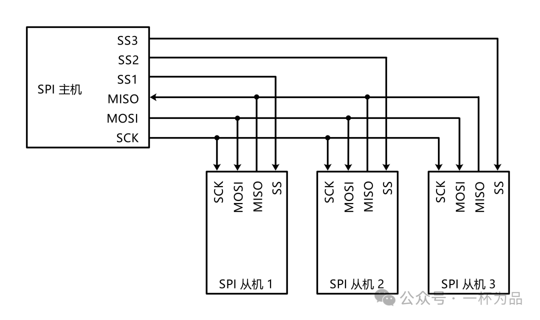
- • All SPI devices’ SCK, MOSI, and MISO are connected together.
- • The master device has multiple SS control lines, each connected to the SS pin of each slave. The SS line is active low; to select a slave, the corresponding SS line must be pulled low. Only one slave can be selected at a time to prevent conflicts.
- • Output pins are configured as push-pull outputs, providing strong high and low level drive, with fast rise and fall times, and transmission speeds far exceeding I2C. However, slave outputs may still conflict, so SPI specifies that unselected slaves must output high-impedance state.
- • Input pins are configured as floating or pull-up inputs.
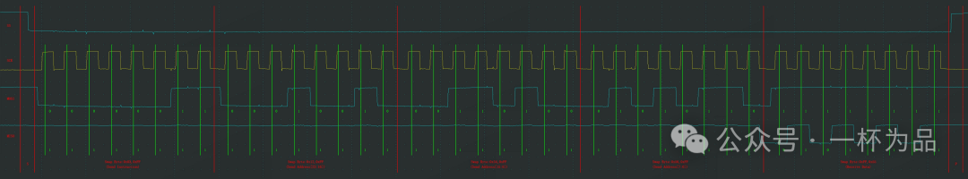
Shift Diagram
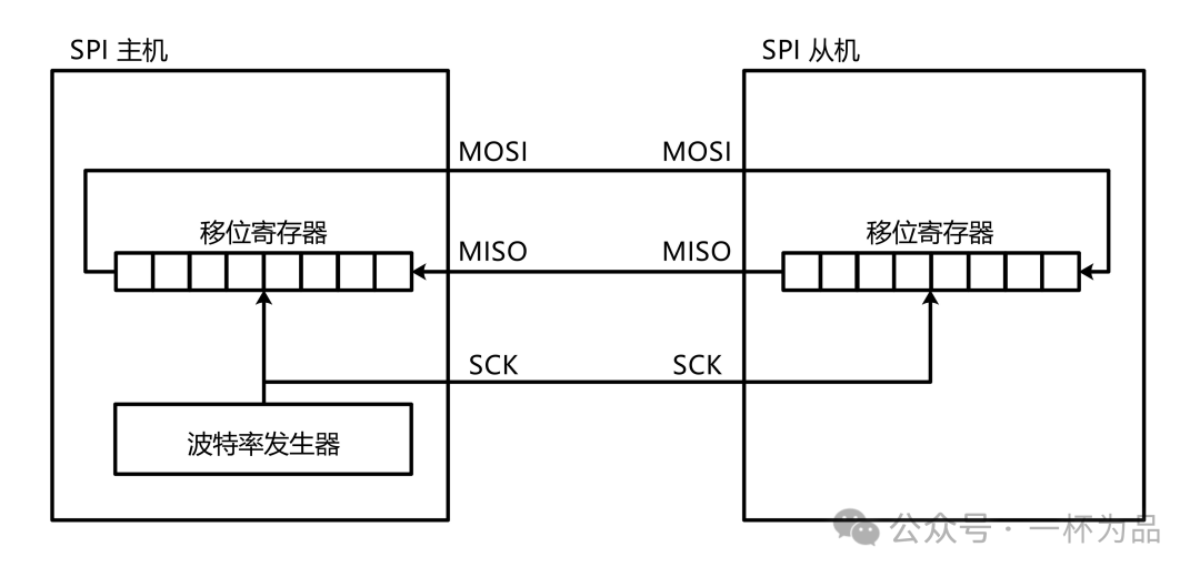
SPI shifts the high bit first, with the clock driving the shift register to shift left. The clock source is provided by the master’s baud rate generator. Data shifted out from the master’s shift register is input to the right end of the slave’s shift register via MOSI, while data shifted out from the slave’s shift register is input to the right end of the master’s shift register via MISO. The rising edge (falling edge) of the baud rate generator drives the shift register to shift out one bit to the pin; the falling edge (rising edge) drives the bit on the pin to be sampled into the least significant bit of the shift register. After eight clock cycles, the master and slave exchange one byte of data, which is the basis of SPI communication. If only sending and not receiving, the master does not read the slave’s input data; if only receiving and not sending, the master can send 0x00 or 0xFF to replace the slave’s data.
Basic Unit of SPI Timing

- • Start condition: SS high → low
- • Stop condition: SS low → high
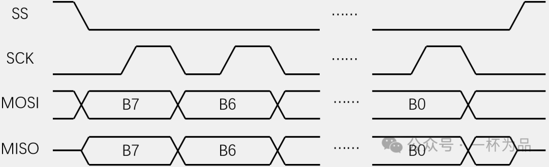
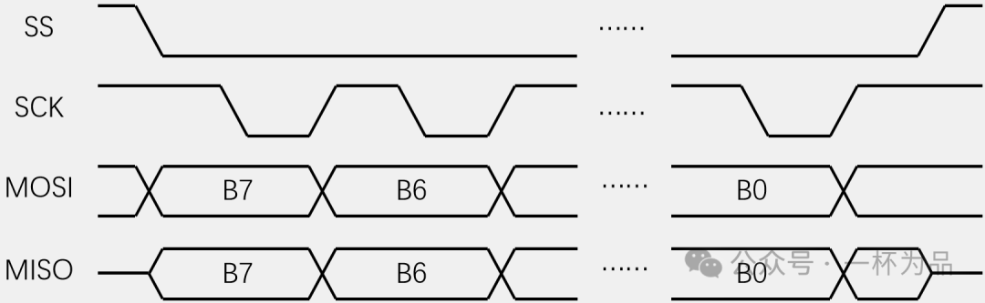
SPI provides two configurable bits in the shift timing for CPOL (Clock Polarity) and CPHA (Clock Phase) to be compatible with more chips. Different configuration combinations form four modes, with mode 0 being the most commonly used.
- • Exchange one byte (Mode 0)
- • CPOL=0: SCK is low in idle state
- • CPHA=0: Data is input on the first edge of SCK (the first edge refers to the edge generated when SCK exits the idle state, which is the rising edge), and data is output on the second edge (the second edge is opposite to the first edge)
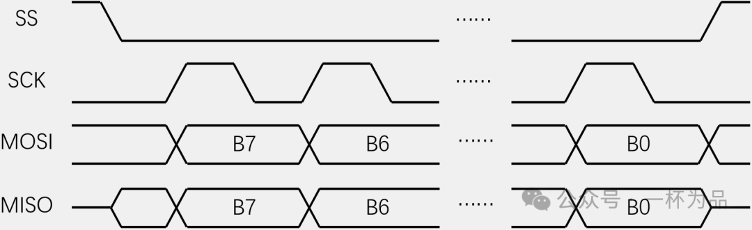
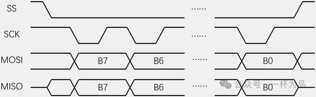
- • Exchange one byte (Mode 1)
- • CPOL=0: SCK is low in idle state
- • CPHA=1: Data is output on the first edge of SCK, and input on the second edge
- • Exchange one byte (Mode 2)
- • CPOL=1: SCK is high in idle state
- • CPHA=0: Data is input on the first edge of SCK, and output on the second edge
- • Exchange one byte (Mode 3)
- • CPOL=1: SCK is high in idle state
- • CPHA=1: Data is output on the first edge of SCK, and input on the second edge
SPI Timing (W25Q64 Chip)
SPI typically uses a command code + read/write data flow, with a command set defined in the slave. After SPI starts, the first data sent to the slave is generally a command code that instructs the slave to perform the corresponding function, followed by continuing to send and receive data as required by the command.
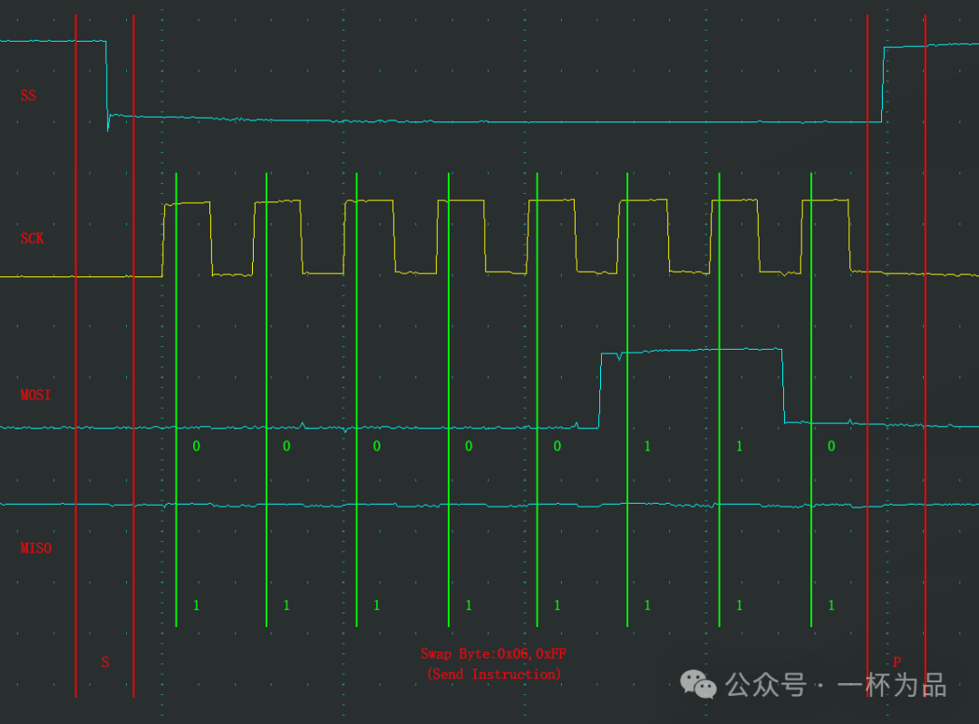
- • Send command
- • Send command (0x06, corresponding to W25Q64 chip write enable command) to the device specified by SS
- • Write to specified address
- • Send write command (0x02) to the device specified by SS, then write specified data (Data, shown as 0x55 in the figure) at the specified address (including three bytes Address[23:0] with high bits first). SPI also has an address pointer that can automatically increment to write multiple bytes continuously.
- • Read from specified address
- • Send read command (0x03) to the device specified by SS, then read data from the slave at the specified address (Address[23:0]) (the master sends 0xFF to replace the slave’s 0x55). Multiple bytes can be read continuously with address auto-increment.
Introduction to W25Q64
- • The W25Qxx series is a low-cost, compact, and easy-to-use non-volatile memory, commonly used in data storage, firmware storage, etc.
- • Storage medium: Nor Flash (Flash memory)
- • Clock frequency: 80MHz/160MHz (Dual SPI)/320MHz (Quad SPI), the latter two use multiple SPI data lines for parallel transmission, just for understanding.
- • The storage capacity of W25Qxx (24-bit address) is xxMbit
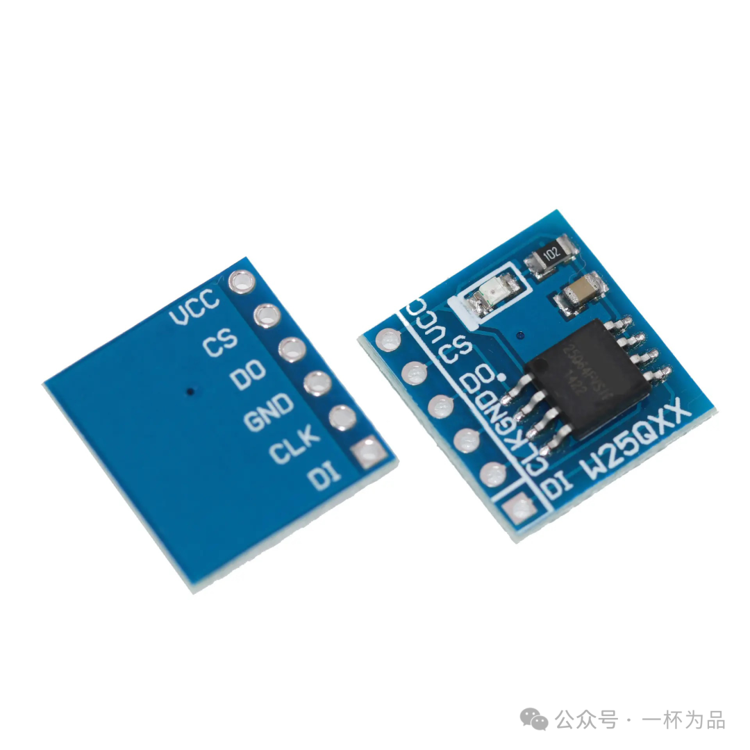
Hardware Circuit
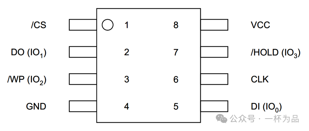
| Pin | Function |
| VCC, GND | Power supply (2.7~3.6V) |
| CS (SS) | SPI chip select |
| CLK (SCK) | SPI clock |
| DI (MOSI) | SPI master output slave input |
| DO (MISO) | SPI master input slave output |
| WP | Write protect |
| HOLD | Data hold |
To release the bus midway, the HOLD pin can be pulled low, and the chip will remember the current timing. To continue with the previous timing, the HOLD pin must be pulled back high.
The IO in parentheses is used as SPI data lines when using dual SPI and quad SPI, just for understanding.
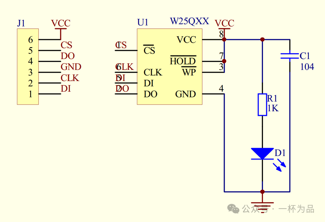
The above figure is the schematic diagram of the W25Qxx module, J1 is the pin header, and D1 is the power indicator.
W25Q64 Block Diagram
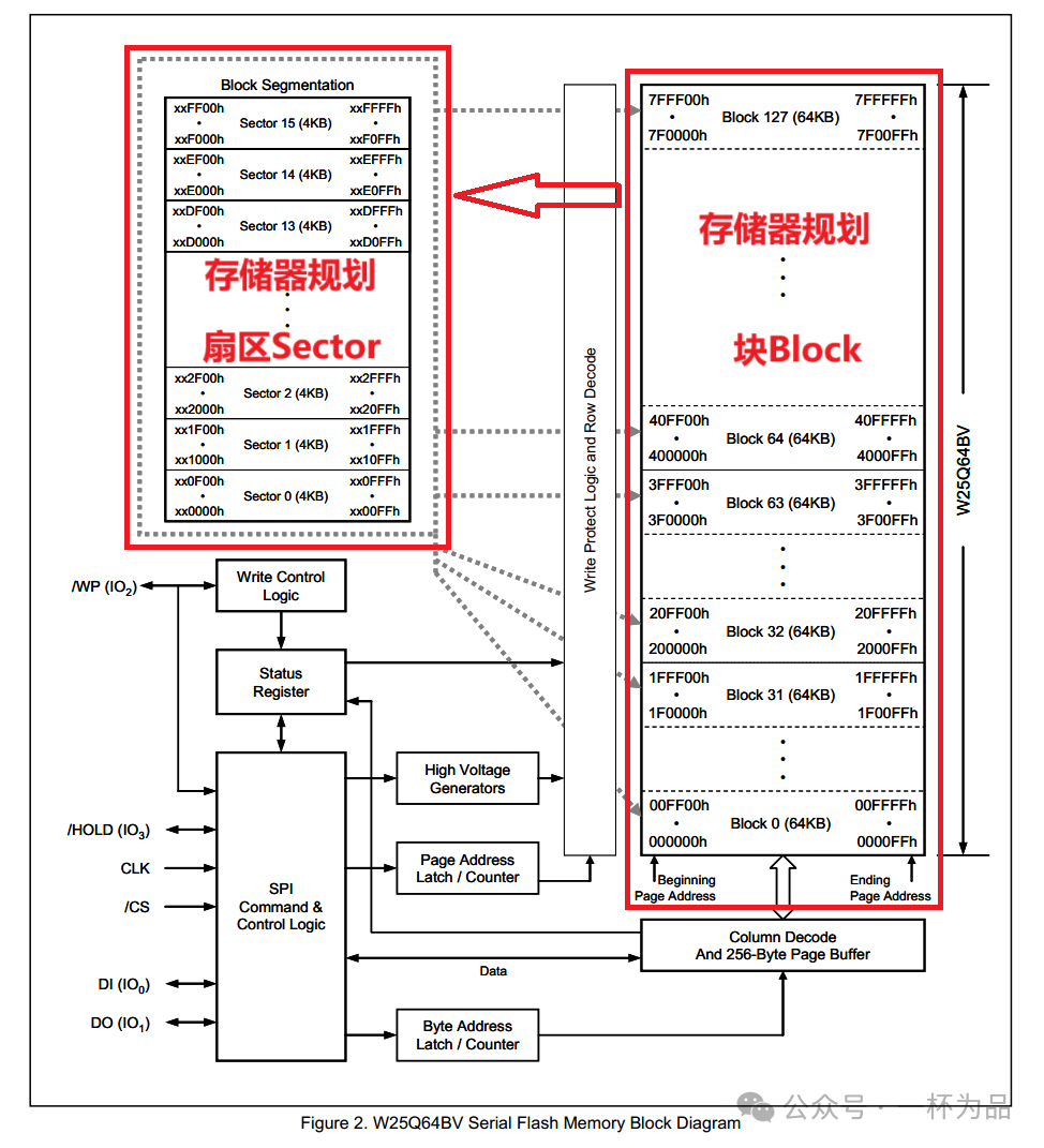
The red box is a schematic diagram of the memory layout, divided into 128×64KB blocks, each block divided into 16×4KB sectors, and each sector divided into 16×256Byte pages. The lower left and upper right corners of each block and sector correspond to the starting and ending addresses, while the left and right ends of the same row of blocks and sectors correspond to the starting and ending addresses of the pages.
The lower left corner contains the SPI control logic (SPI Command & Control Logic), which automatically completes address latching and data read/write operations. The left side of the control logic connects to the communication pins with the main control chip, which sends commands and data to the control logic via the SPI protocol, and the control logic automatically operates the internal circuits to complete the corresponding functions. Above the control logic is the status register (Status Register), which relates to busy status, write enable/protect, and will be detailed later. Above that is the write control logic (Write Control Logic) that implements write protection in conjunction with the WP pin. To the right of the SPI control logic is the high voltage generator (High Voltage Generator), which works with Flash for programming, ensuring data retention during power loss; the page/byte address latch/counter (Page/Byte Address Latch/Counter) is used to specify addresses, with the first two bytes of the three-byte address entering the page address latch/counter, and the last byte entering the byte address latch/counter. The page address is selected for operation through write protection and row decoding (Write Protect Logic & Row Decode), while the byte address is specified through column decoding and the 256-byte page buffer (Column Decode & 256-Byte Page Buffer) for read/write operations. Data is first stored in the page buffer to keep up with SPI transmission speed, and after writing is complete (continuous writing not exceeding 256 bytes), the chip transfers the data from the buffer to Flash memory, at which point the chip enters a busy state, setting the BUSY bit in the status register to 1, and will not respond to new read/write timings. The counter automatically increments the address pointer after read/write operations.
Flash Operation Considerations
To achieve non-volatility during power loss while ensuring sufficient storage capacity and low cost, Flash memory has made compromises in operational convenience.
Write Operation
- • Before a write operation, write enable must be performed.
- • Each data bit can only be rewritten from 1 to 0, not from 0 to 1.
- • To compensate for the previous limitation, data must be erased before writing, which sets all data bits to 1.
- • Erasure must be performed according to the minimum erase unit (one sector); if some bytes need to be retained, they must be read as a backup first.
- • Due to the existence of the page buffer, when writing multiple bytes continuously, a maximum of 256 bytes can be written from the starting position; data exceeding the page end will wrap around and overwrite from the page start.
- • After the write operation is complete, the chip enters a busy state and does not respond to new read/write operations; it can only be performed when the BUSY bit in the status register is 0.
Read Operation
- • Directly call the read timing, no need for enable, no additional operations, no page restrictions; the read operation does not enter a busy state after completion, but cannot read while in a busy state.
Status Register
The W25Q64 has two status registers, but we only focus on the first two bits of the important status register 1. The first bit is the BUSY bit mentioned earlier, and the second bit is the write enable latch bit WEL. After executing the write enable command, WEL is set to 1, indicating that the chip can perform write operations. Write disable will clear WEL to 0; powering on the chip, executing write disable, page programming, and erase commands will trigger write disable, so write enable must be performed before any write operation.
Instruction Set
The experiment involves the following commands:
| Function | Command | Data |
| Write Enable | 0x06 | |
| Write Disable | 0x04 | |
| Read Status Register 1 | 0x05 | Exchange to read one byte of status register 1 configuration |
| Page Programming (Write Data) | 0x02 | Write three-byte address and one-byte dataSubsequent bytes are stored sequentially with address auto-increment |
| Sector Erase | 0x20 | Write three-byte address |
| Read JEDEC ID | 0x9F | Exchange three-byte ID (one-byte manufacturer ID + two-byte device ID) |
| Read Data | 0x03 | Write three-byte address, exchange to read one byte of dataSubsequent bytes are read sequentially with address auto-increment |
Experiment 26 Software SPI Read/Write W25Q64
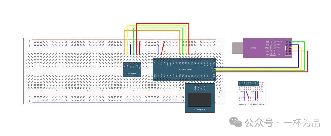
Wiring Diagram
SPI Protocol Layer
MySPI.h
#ifndef __MYSPI_H
#define __MYSPI_H

void MySPI_Init(void);
void MySPI_Start(void);
void MySPI_Stop(void);
uint8_t MySPI_SwapByte(uint8_t ByteSend);

#endif
MySPI.c
#include "stm32f10x.h"

// Encapsulate output pin write
void MySPI_W_SS(uint8_t BitValue)
{
    GPIO_WriteBit(GPIOA, GPIO_Pin_4, (BitAction)BitValue);
}

void MySPI_W_SCK(uint8_t BitValue)
{
    GPIO_WriteBit(GPIOA, GPIO_Pin_5, (BitAction)BitValue);
}

void MySPI_W_MOSI(uint8_t BitValue)
{
    GPIO_WriteBit(GPIOA, GPIO_Pin_7, (BitAction)BitValue);
}

// Encapsulate input pin read
uint8_t MySPI_R_MISO(void)
{
    return GPIO_ReadInputDataBit(GPIOA, GPIO_Pin_6);
}

void MySPI_Init(void)
{
    RCC_APB2PeriphClockCmd(RCC_APB2Periph_GPIOA, ENABLE);
    // Except MISO as pull-up input, others as push-pull output
    GPIO_InitTypeDef GPIO_InitStructure;
    GPIO_InitStructure.GPIO_Mode = GPIO_Mode_Out_PP;
    GPIO_InitStructure.GPIO_Pin = GPIO_Pin_4 | GPIO_Pin_5 | GPIO_Pin_7;
    GPIO_InitStructure.GPIO_Speed = GPIO_Speed_50MHz;
    GPIO_Init(GPIOA, &GPIO_InitStructure);
    GPIO_SetBits(GPIOA, GPIO_Pin_4 | GPIO_Pin_5 | GPIO_Pin_7);
    GPIO_InitStructure.GPIO_Mode = GPIO_Mode_IPU;
    GPIO_InitStructure.GPIO_Pin = GPIO_Pin_6;
    GPIO_InitStructure.GPIO_Speed = GPIO_Speed_50MHz;
    GPIO_Init(GPIOA, &GPIO_InitStructure);
    GPIO_SetBits(GPIOA, GPIO_Pin_6);

    // Initialize pin default levels
    // Not selecting slave
    MySPI_W_SS(1);
    // Mode 0 clock idle low
    MySPI_W_SCK(0);
}

// Start signal
void MySPI_Start(void)
{
    MySPI_W_SS(0);
}

// Stop signal
void MySPI_Stop(void)
{
    MySPI_W_SS(1);
}

// Swap byte (Mode 0)
uint8_t MySPI_SwapByte(uint8_t ByteSend)
{
    uint8_t i, ByteReceive = 0x00;
    for(i = 0;i < 8;i++)
    {
        // Software cannot execute two statements simultaneously, so first generate edge then operate data
        MySPI_W_MOSI(ByteSend & (0x80 >> i));
        MySPI_W_SCK(1);
        // Rising edge inputs byte
        if(MySPI_R_MISO())ByteReceive |= (0x80 >> i);
        MySPI_W_SCK(0);
        // Falling edge outputs byte (back to loop start)
    }
    // If using other modes
    // Change polarity then swap clock write 1 and write 0 statements
    // Change phase then advance clock to before read/write operation
    return ByteReceive;
}
W25Q64 Driver Layer
W25Q64.h
#ifndef __W25Q64_H
#define __W25Q64_H

void W25Q64_Init(void);
void W25Q64_ReadID(uint8_t *MID, uint16_t *DID);
void W25Q64_PageProgram(uint32_t Address, uint8_t *DataArray, uint16_t Count);
void W25Q64_SectorErase(uint32_t Address);
void W25Q64_ReadData(uint32_t Address, uint8_t *DataArray, uint32_t Count);

#endif
W25Q64.c
#include "stm32f10x.h"
#include "MySPI.h"
#include "W25Q64_Ins.h"

void W25Q64_Init(void)
{
    MySPI_Init();
}

// Read JEDEC ID, pointer implementation for multiple return parameters, MID manufacturer ID, DID device ID
void W25Q64_ReadID(uint8_t *MID, uint16_t *DID)
{
    MySPI_Start();
    // Command
    MySPI_SwapByte(W25Q64_JEDEC_ID);
    // Replace ID data
    *MID = MySPI_SwapByte(W25Q64_DUMMY_BYTE);
    // DID high eight bits first then low eight bits
    *DID = MySPI_SwapByte(W25Q64_DUMMY_BYTE);
    *DID <<= 8;
    *DID |= MySPI_SwapByte(W25Q64_DUMMY_BYTE);
    MySPI_Stop();
}

// Write enable, used at the beginning of page programming and sector erase
void W25Q64_WriteEnable(void)
{
    MySPI_Start();
    MySPI_SwapByte(W25Q64_WRITE_ENABLE);
    MySPI_Stop();
}

// Wait for BUSY, used at the end of page programming and sector erase
void W25Q64_WaitBusy(void)
{
    MySPI_Start();
    MySPI_SwapByte(W25Q64_READ_STATUS_REGISTER_1);
    // Wait for the lowest bit BUSY in status register 1 to clear
    while((MySPI_SwapByte(W25Q64_DUMMY_BYTE) & 0x01) == 0x01);
    MySPI_Stop();
}

// Page programming
// Parameters are address (C language uses 32 bits instead of 24 bits), byte array, number of bytes to write (0-256 using 16 bits)
void W25Q64_PageProgram(uint32_t Address, uint8_t *DataArray, uint16_t Count)
{
    uint16_t i;
    W25Q64_WriteEnable();
    MySPI_Start();
    MySPI_SwapByte(W25Q64_PAGE_PROGRAM);
    // High bits first, after shifting the program automatically receives the low eight bits
    MySPI_SwapByte(Address >> 16);
    MySPI_SwapByte(Address >> 8);
    MySPI_SwapByte(Address);
    // Write data
    for(i = 0;i < Count;i++)
    {
        MySPI_SwapByte(DataArray[i]);
    }
    MySPI_Stop();
    W25Q64_WaitBusy();
}

// Sector erase
void W25Q64_SectorErase(uint32_t Address)
{
    W25Q64_WriteEnable();
    MySPI_Start();
    MySPI_SwapByte(W25Q64_SECTOR_ERASE_4KB);
    MySPI_SwapByte(Address >> 16);
    MySPI_SwapByte(Address >> 8);
    MySPI_SwapByte(Address);
    MySPI_Stop();
    W25Q64_WaitBusy();
}

// Read data
// Count is unlimited, give maximum type
void W25Q64_ReadData(uint32_t Address, uint8_t *DataArray, uint32_t Count)
{
    uint32_t i;
    MySPI_Start();
    MySPI_SwapByte(W25Q64_READ_DATA);
    MySPI_SwapByte(Address >> 16);
    MySPI_SwapByte(Address >> 8);
    MySPI_SwapByte(Address);
    for(i = 0;i < Count;i++)
    {
        DataArray[i] = MySPI_SwapByte(W25Q64_DUMMY_BYTE);
    }
    MySPI_Stop();
}
Main Program
#include "stm32f10x.h"
#include "Delay.h"
#include "OLED.h"
#include "W25Q64.h"

uint8_t MID;
uint16_t DID;
// Write array
uint8_t ArrayWrite[] = {0x01, 0x02, 0x03, 0x04};
uint8_t ArrayRead[4];

int main(void)
{
    OLED_Init();
    W25Q64_Init();

    OLED_ShowString(1, 1, "MID:   DID:");
    OLED_ShowString(2, 1, "W:");
    OLED_ShowString(3, 1, "R:");

    W25Q64_ReadID(&MID, &DID);

    OLED_ShowHexNum(1, 5, MID, 2);
    OLED_ShowHexNum(1, 12, DID, 4);
    // Erase before writing, address should be aligned to sector starting address (low three bits are 000)
    W25Q64_SectorErase(0x000000);
    W25Q64_PageProgram(0x000000, ArrayWrite, 4);
    W25Q64_ReadData(0x000000, ArrayRead, 4);

    OLED_ShowHexNum(2, 3, ArrayWrite[0], 2);
    OLED_ShowHexNum(2, 6, ArrayWrite[1], 2);
    OLED_ShowHexNum(2, 9, ArrayWrite[2], 2);
    OLED_ShowHexNum(2, 12, ArrayWrite[3], 2);
    OLED_ShowHexNum(3, 3, ArrayRead[0], 2);
    OLED_ShowHexNum(3, 6, ArrayRead[1], 2);
    OLED_ShowHexNum(3, 9, ArrayRead[2], 2);
    OLED_ShowHexNum(3, 12, ArrayRead[3], 2);
    while(1)
    {
    }
}