GaN Epitaxy—— The Art of Heterogeneous Integration Growth

Gallium Nitride (GaN) is a new generation of wide bandgap semiconductor material, known for itshigh breakdown electric field (>3 MV/cm),high electron mobility (>1500 cm²/V·s), and high saturation electron drift velocity, which are rapidly reshaping the device boundaries in power electronics, high-frequency communications, and RF microwave technologies. In the fields of5G base stations, high-end fast charging, radar communication, and satellites, the superiority of GaN devices has been clearly validated. However, the key to whether GaN devices can truly achieve large-scale commercial deployment lies not only in the superior performance of the material itself but also in itsepitaxial structure’s “implementation capability”.
Traditional GaN devices primarily use sapphire or SiC as substrates for epitaxial growth. Although the lattice compatibility is good, the high cost of the materials severely limits their application in consumer-grade and high-throughput fields. For typical parameters,6 inch SiC substrate prices are about50 USD/cm², while sapphire prices are around15 USD/cm², which, while ensuring lattice matching and thermal stability, also raises the overall manufacturing costs. In contrast, the GaN-on-Si epitaxial structure provides the industry with a “balance lever between performance and cost”: leveraging the low cost, high size compatibility, and CMOS process integration of the mature silicon industry chain, GaN-on-Si structure devices have already shown mass production potential on6 inch,8 inch, and even12 inch platforms, maintaining over80% of performance while reducing the single wafer cost by nearly60%, achieving a fivefold industrial leap in performance in high-frequency, high-power, and broadband communication scenarios.
However, the significant differences in lattice and thermal expansion coefficients between silicon and GaN also bring unprecedented epitaxial challenges.GaN and Si have a lattice mismatch of up to16%, far exceeding the stress tolerance threshold of typical III-V semiconductor hetero-systems. This mismatch directly induces dislocations, cracks, warping, and delamination, severely restricting the integrity of the epitaxial structure and the reliability of the devices. To address this, the industry commonly introduces AlN or AlGaN buffer layers as transition structures to absorb stress, regulate thermal flow, and improve crystal quality. However, even so, controlling the dislocation density below10⁸/cm², suppressing crack propagation and warping evolution, and constructing high-quality multi-quantum well structures (MQWs) in high-stress fields remain key scientific and engineering challenges that restrict the true industrialization of silicon-based GaN.
It is against this backdrop that GaN epitaxy has evolved from a single material growth to a cross-disciplinary, cross-platform, and cross-structure “art of heterogeneous integration”. From stress compensation layer design to selective epitaxy windows, from high-temperature metal-organic chemical vapor deposition (MOCVD) optimization to nanoscale interface control strategies, and then to multi-quantum well (MQW) structure band engineering and dislocation passivation mechanisms, a complete set of innovative systems based on material physics as the underlying logic, structural coupling as the engineering foundation, and industrial adaptation as the target is rapidly being constructed.
This article will focus on the core technologies and structural strategies in GaN epitaxy, sequentially discussing heterogeneous substrate adaptation mechanisms, buffer layer design evolution, and the synergistic logic of multi-quantum wells and stress engineering, combined with the layout and industrialization paths of domestic and foreign enterprises for a comprehensive analysis, revealing how silicon-based GaN heterostructures transition from “lattice confrontation” to “symbiotic harmony”, achieving the true popularization of wide bandgap devices.
1. Epitaxial Growth Methodology: The Game and Evolution of Three Technologies
In the technical landscape of GaN materials, epitaxial growth is the key bridge connecting material physics and device structure, determining the material quality, device performance, and process compatibility, serving as the “source process”. However, the growth of gallium nitride is not a traditional “unidirectional deposition”, but a complex multidimensional game of thermodynamics, kinetics, interface physics, and reaction chemistry. Especially under heterogeneous substrate conditions (such as GaN-on-Si), the film formation mechanisms, stress responses, and defect control capabilities exhibited by different epitaxial methods directly determine the design freedom of subsequent devices and the process window of production lines.
The mainstream GaN epitaxial technologies currently include metal-organic chemical vapor deposition (MOCVD), molecular beam epitaxy (MBE), and hydride vapor phase epitaxy (HVPE), each with its own advantages and disadvantages in growth rate, temperature control capability, defect density, and cost structure. From an industrial practice perspective,MOCVD has become the mainstream manufacturing path for GaN devices due to its overall optimal process characteristics, while MBE and HVPE maintain certain technical barriers in ultra-thin film growth and large-volume template transfer, respectively.
In terms of growth rate, HVPE has an overwhelming advantage, with typical rates reaching100 μm/h, far exceeding MOCVD’s 2.0 μm/h and MBE’s 0.3 μm/h, but its vigorous gas-phase reactions and difficult doping control make it challenging to achieve precise control of multi-quantum well (MQW) structures, making it more suitable for photovoltaic devices or rapid preparation of large-size sapphire templates. MBE, while possessing atomic-level layer control capability and excellent interface flatness, faces inherent bottlenecks in high-temperature stress adjustment and thick film deposition due to its low growth temperature and inefficient reaction, limiting its application expansion in large-scale power devices.
The reason MOCVD has established its dominant position in high-frequency devices and industrial applications is due to its comprehensive advantages in temperature control, reaction uniformity, and doping precision. Taking the current mainstream dual gas flow reactor design as an example, by optimizing the gas atmosphere ratio of H₂/N₂=3:1, the reaction rate and boundary layer thickness can be controlled, achieving film thickness uniformity control within ±1.5% (as represented by the mass production data of Royole Technology). At the same time, the high-end MOCVD systems equipped with AI temperature control systems that utilize 300 thermocouples for real-time feedback on thermal field distribution, combined with multidimensional PID algorithms to adjust heating areas, can achieve a thermal spot elimination rate of over 95%, greatly improving the stress concentration issues caused by temperature gradients in large-size substrates (such as 6 inch silicon).
In terms of defect control, the three epitaxial methods form a performance gradient: HVPE initially forms thick film templates with dislocation densities as low as 10⁶/cm², suitable for subsequent peeling transfer and re-epitaxy; MBE generally has a dislocation density around 10⁸/cm² due to its low-energy deposition mechanism, mostly penetrating type; while MOCVD has now stabilized the dislocation density control below 5×10⁷/cm² through optimization of AlN/AlGaN multilayer buffer structures, three-step temperature rise methods, and low-temperature nucleation island strategies, meeting the application needs of RF, radar, etc., which have higher defect tolerance but are cost-sensitive.
From a cost structure perspective, HVPE equipment is relatively simple, and the precursor cost is low, forming a cost index of only 0.8, but its equipment safety is poor, and the epitaxial quality is unstable, making it difficult to meet the reliability requirements for mass production of commercial GaN devices; MBE equipment is complex, energy-intensive, and has strict vacuum requirements, with a cost index as high as 3.5, retaining advantages only in research and special microstructure growth. In contrast, MOCVD maintains an engineering balance point at a cost index of 1.0, building a stable and sustainable industrial system, and forming mass production capabilities in various subfields such as optical communication, radar systems, GaN fast charging modules, and high-frequency PA chips.
In summary, MOCVD represents the main path of GaN epitaxy technology, while MBE and HVPE provide beneficial supplements in constructing special fine structures and template-level epitaxy, respectively. The relationship between the three processes is not simply one of superiority or inferiority, but rather a differentiated division of labor formed under different substrates, structures, and application scenarios. The future technological evolution path will emphasize integrated solutions of multi-process fusion to adapt to the complex scenario requirements of heterogeneous integration and multi-structure epitaxy.
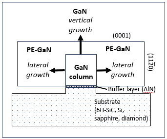
Pendeo Epitaxy (PE) growth schematic of GaN, Wikipedia
2. Growth Modes and Defect Engineering: The Path to Overcoming Lattice Mismatch
In the panoramic view of GaN epitaxy technology, lattice mismatch and thermal mismatch are the core obstacles in the path of heterogeneous integration. Taking silicon substrates as an example, there is a lattice constant difference of up to 16% and a significant thermal expansion coefficient mismatch between GaN, which can easily induce dislocations, cracks, warping, and film delamination during high-temperature growth and cooling processes. To achieve high-quality GaN epitaxial layers, the industry has undergone multiple rounds of engineering iterations from material systems, interlayer structures to doping mechanisms, gradually forming a relatively mature defect passivation and strain control strategy system.
First, in terms of buffer layer structure design, traditional single-layer AlN has gradually evolved towards multi-stage stress transition structures. The most representative is the introduction of gradient composition AlGaN buffer layers. By gradually adjusting the aluminum content in AlGaN during the epitaxy process from 80% to 20%, strain can be released in a gradient along the thickness direction, effectively alleviating the sudden concentration of lattice tension. This strain modulation design not only reduces the excitation probability of dislocation sources but also forms elastic buffer zones between layers, effectively controlling dislocation density below 10⁷/cm², significantly enhancing material integrity and surface flatness, and is one of the widely adopted engineering methods in current MOCVD equipment.
On this basis, some high-end device manufacturing paths have also introduced nano-patterned substrates (NPSS) technology, which constructs periodic nano-structures on the substrate surface through physical or chemical methods, inducing preferential epitaxy of the lattice along specific orientations. For example, a silicon dioxide nano-pillar array with a diameter of about 200 nm can not only disperse stress concentration areas and suppress the propagation of penetrating dislocations but also enhance reflection and scattering effects in optoelectronic devices, significantly improving light extraction efficiency. In specific LED structures, the GaN epitaxial layer achieved through NPSS can improve quantum efficiency by about 35%, becoming one of the core processes for high-brightness lighting and micro-displays.
In addition to structural optimization, breakthroughs in doping strategies also determine the electrical performance and functional realization of GaN devices, especially p-type doping, which has long been considered the “Achilles’ heel” of wide bandgap semiconductor development. Due to the extremely low hole activation rate of Mg doped in GaN (about 1%), and its susceptibility to hydrogen passivation, traditional continuous doping methods struggle to achieve efficient hole conduction. Therefore, advanced MOCVD systems have introduced pulsed doping mechanisms (Pulsed Doping): by controlling the opening cycle of the Mg source, periodic Mg injection on the order of 0.5 seconds can be achieved, maintaining short-term high concentration and high coverage local doping within each cycle, effectively avoiding Mg source diffusion and residual effects in the reaction chamber. Measurements show that under this method, the GaN film’s hole concentration can reach 5×10¹⁷ cm⁻³, about twice that of traditional continuous doping, significantly enhancing the conductivity and carrier uniformity of the p-type layer.
Furthermore, to further activate p-type carriers, low-temperature rapid annealing processes have become a key complementary step. Unlike traditional high-temperature long-duration annealing, modern equipment generally adopts 700℃, 2 minutes rapid annealing processes, which can effectively break the hydrogen passivation effect in Mg-H complexes (with a passivation removal rate of up to 90%), while avoiding Mg diffusion and interlayer reactions under high-temperature conditions, maintaining the stability of film structure and doping distribution. This doping-annealing synergistic scheme has been successfully validated in fast-charging GaN devices, high-frequency PA chips, and RF-SOI modules, providing solid support for the high performance of p-type GaN structures.
In summary, through diversified technical synergies such as gradient AlGaN buffer design, nano-patterned substrate-induced growth, pulsed doping control, and low-temperature annealing activation, the lattice adaptability and carrier characteristics of GaN epitaxy have been significantly optimized. Epitaxy is no longer just a physical stacking process, but a “material art engineering” that reshapes barriers and energy bands, stress and interfaces at the lattice scale, with complexity and refinement comparable to any cutting-edge device construction logic.
3. Cutting-edge Structure Design: From Power Devices to Quantum Light Sources
The true application value of GaN materials lies not only in the growth quality of the epitaxial layer but also in the engineering feasibility of a series of high-performance device structures. From high electron mobility transistors (HEMT) in RF high-frequency fields to micro-nano quantum light-emitting devices (such as nanowire LEDs and quantum dot light-emitting structures) in emerging information photonics technology, the evolution of GaN epitaxial systems has penetrated into every structural detail of device physics, energy band engineering, and even quantum control, initiating a deep leap from “crystal quality optimization” to “functional structure integration”.
In the field of power devices, the HEMT structure is the most representative carrier for high-frequency and high-voltage applications of GaN. This structure induces the formation of a two-dimensional electron gas (2DEG) channel that is not limited by ionization scattering by constructing heterojunction interfaces (such as AlGaN/GaN or AlN/GaN), achieving high carrier capacity and reliability even under extreme conditions. For typical parameter comparisons, the 2DEG density in the AlGaN/GaN structure can reach 1.2×10¹³ cm⁻², with an electron mobility of about 2000 cm²/V·s, and a breakdown voltage of up to 650 V, widely used in 5G RF power amplifiers and high-frequency DC-DC conversion modules. Under higher performance demands, using AlN/GaN heterostructures can further enhance the interface barrier, with the 2DEG density rising to 2.5×10¹³ cm⁻², and the breakdown voltage breaking through to 1200 V, although the mobility slightly decreases to 850 cm²/V·s due to interface roughness and enhanced polarization fields, it still shows great potential in millimeter-wave radar and aerospace communications.
To further enhance device stability and switching speed, surface passivation technology has become a key process. Unpassivated GaN surfaces are prone to generate interface state traps, inducing current collapse phenomena that severely affect power output and waveform stability. The current mainstream approach is to deposit a SiNₓ dielectric film with a thickness of about 30 nm after epitaxy (commonly using plasma-enhanced CVD processes), which can effectively shield interface traps and leakage channels, improving the current collapse suppression rate to over 80%. This process has been widely applied in GaN-on-Si HEMT device platforms of institutions such as China Electronics Technology Group Corporation and the Institute of Microelectronics, Chinese Academy of Sciences.
In the field of micro-nano optoelectronic devices, GaN materials are also entering a new stage of “quantization” engineering, especially with new light-emitting architectures represented by nanowire LEDs and quantum dot structures, opening up higher-dimensional space for GaN in cutting-edge fields such as micro-displays, tunable lasers, and quantum communication. Typical nanowire LEDs adopt VLS (vapor-liquid-solid) or selective area epitaxy methods, forming high aspect ratio nano-pillar arrays through self-assembly on substrates, introducing InGaN quantum dot structures (with a diameter of about 5 nm), which can achieve strong binding effects of electron-hole pairs in extremely small volumes, significantly enhancing radiative recombination efficiency. Compared to traditional planar structure LEDs, their internal quantum efficiency has increased from 70% to 92%, greatly suppressing non-radiative recombination and waveguide mode losses.
To achieve higher light extraction capabilities, micro-nano LEDs also integrate micro-cavity enhancement structure designs. The most typical is the introduction of distributed Bragg reflectors (DBR) as reflectance enhancers for vertical cavities, using alternating deposition of TiO₂/SiO₂ with 15 pairs of high and low refractive index layers, constructing high reflectivity grids. The reflectivity of this structure at the target wavelength can reach over 98%, enhancing the overall light extraction efficiency to 78%, especially suitable for UV-LED and micro-laser platforms.
Overall, from the design of two-dimensional channels in high-voltage devices to quantum-scale control of light-emitting structures, GaN epitaxy technology is transitioning from a material platform to device integration dominance, with the collaborative construction of different heterojunction schemes, doping strategies, and optical structures not only extending epitaxial capabilities but also redefining material potential. It marks the entry of wide bandgap semiconductors into a new logical era of “structure equals performance”: epitaxy is no longer just pure material growth, but an integrated control of functional structures and energy bands.
4. Industry-Academia-Research Ecosystem Map: Technology Transfer and Domestic Challenges
The iteration of GaN epitaxy technology relies not only on the continuous optimization of basic materials and processes but is also deeply rooted in an industry-academia-research ecosystem that forms a closed loop from universities— research institutions— enterprises— end markets. Unlike traditional silicon-based industries, breakthroughs in GaN epitaxy technology often rely on the close collaboration of high-precision material engineering and equipment processes, making its commercialization process highly dependent on cross-institutional collaboration and international technology transfer mechanisms. Globally, a number of key technology platforms and representative cases of industrialization have become the leading edge for GaN epitaxy to transition from laboratory to large-scale production.
In the UK, the University of Cambridge has promoted the commercial transformation of high-quality GaN epitaxial layers in the micro-lighting field through long-term research on nano-patterned substrate (NPSS) technology. Its technology has achieved mass production through collaboration with the company IQE and has been used in some models of Apple’s UV sensor chips, becoming one of the representative symbols of GaN’s industrial landing in the consumer electronics field. This case not only demonstrates a rapid migration path from academic frontiers to industrial applications but also reflects the core driving role of epitaxial structure innovation on terminal performance.
China has also formed a representative industry-academia-research collaborative model in the industrialization of GaN epitaxy. Taking the Suzhou Institute of Nano-Tech and Nano-Bionics, Chinese Academy of Sciences as an example, it has made significant breakthroughs in the ohmic contact technology of p-type GaN layers, solving key bottlenecks of high contact resistance and poor reliability that have long existed in GaN devices. This achievement has been directly transformed into the Inno-Silicon 8-inch GaN-on-Si industrial production line and is widely used in the mobile phone fast charging chip market, currently achieving over 40% market share among mid-to-high-end brands, marking that China has the capability to compete with international players in certain subfields of wide bandgap devices.
In the United States, the Massachusetts Institute of Technology (MIT) has established a technical barrier for precise control of ultra-thin layers by developing atomic layer epitaxy (ALE) processes, especially suitable for the growth of high-frequency low-loss GaN RF structures. This technology has been integrated into TSMC’s GaN-on-Si foundry platform, achieving bulk supply of power amplifier modules (PA) required for 5G base stations, reflecting the efficient linkage capability between cutting-edge academic research and advanced manufacturing enterprises.
However, compared to the complete epitaxy-device-packaging industrial chain controlled by international giants, China still faces multiple domestic challenges and structural bottlenecks in the GaN epitaxy industry ecosystem. The first is a serious reliance on core equipment: currently, China is still highly dependent on imports for key epitaxy equipment, especially theMOCVD equipment’s domestic production rate is still below 20%. Although companies like Micro Semiconductor have made breakthroughs in the design of 12-inch reaction chambers and temperature field uniformity control, there are still significant gaps in control software, reaction chamber materials, and multi-chamber coordination, leading to high-end epitaxy process equipment still relying on imported tools.
Secondly, the lagging standard system and long reliability verification cycles. Especially in automotive-grade applications (such as new energy vehicle radar, OBC systems), GaN devices need to meet high reliability certification standards such as AEC-Q101, which requires over 2000 hours of high-temperature reverse bias and power thermal cycling tests, posing a high-cost entry barrier for domestic manufacturers still in the ramp-up phase. In addition, in areas such as failure rate assessment, thermal stability indicators, and electromagnetic compatibility ( EMC) testing, China’s standard system lags behind international standards such as SEMI and JEDEC by 2-3 years, further limiting the certification adaptation and export layout of domestic devices in the global market.
Overall, the industrialization of GaN epitaxy technology has transitioned from single-point breakthroughs to the stage of structured platform building. From material innovation in research institutions to large-scale production in enterprises, and rapid penetration into terminal applications, a positive feedback path characterized by structural optimization—process integration—application feedback is forming. However, to truly achieve technological independence and supply chain security, continuous efforts are still needed in areas such as domestic production of core equipment, standard system construction, and the cultivation of platform-type enterprises to build a competitive wide bandgap semiconductor ecosystem.
 You’ve read this far, why not follow us?
-
Tzou, A.-J., Chu, K.-H., Lin, I.-F., Østreng, E., Fang, Y.-S., Wu, X.-P., … Kuo, H.-C. (2017). AlN surface passivation of GaN-based high electron mobility transistors by plasma-enhanced atomic layer deposition. Nanoscale Research Letters, 12, 315. (pmc.ncbi.nlm.nih.gov)
-
Zhang, et al. (2021). Improved electrical properties of AlGaN/GaN high-electron-mobility transistors by in situ tailoring the SiNₓ passivation layer. ACS Applied Materials & Interfaces, 13(15), 18264–18273. (pubs.acs.org)
-
Ambacher, O., et al. (2000). Two‑dimensional electron gases induced by spontaneous and piezoelectric polarization in undoped and doped AlGaN/GaN heterostructures. Journal of Applied Physics. (reddit.com)
-
Ibbetson, J. P., et al. (2000). Polarization effects, surface states, and the source of electrons in AlGaN/GaN heterostructure field effect transistors. Applied Physics Letters. (reddit.com)
-
Vetury, R., et al. (2001). The impact of surface states on the DC and RF characteristics of AlGaN/GaN HFETs. IEEE Transactions on Electron Devices, 48(3), 560–567. (reddit.com)
-
Meneghini, M., De Santi, C., Abid, I., Buffolo, M., & Cioni, M. (n.d.). GaN-based power devices: Physics, reliability, and perspectives. Journal of Applied Physics. (en.wikipedia.org)
-
Works on AlGaN buffer engineering on Si: Design of step‑graded AlGaN buffers for GaN‑on‑Si heterostructures grown by MOCVD. IOP Materials Research. (iopscience.iop.org)
-
Studies on GaN buffer layers on SiC: Effect of two‑step GaN buffer on structural and electrical characteristics in AlGaN/GaN heterostructure. Vacuum, 178, 109442 (2020). (sciencedirect.com)
-
RSC Publication (2024). AlN interlayer‑induced reduction of dislocation density in the AlGaN epilayer. CrystEngComm. (pubs.rsc.org)
-
Applied Physics Letters (1997). Thermal mismatch stress relaxation via lateral epitaxy in selectively grown GaN structures. (en.wikipedia.org)
-
Wikipedia contributors. (2025). High-electron-mobility transistor. In Wikipedia, The Free Encyclopedia. Retrieved April 2025. (en.wikipedia.org)