
Content from: Jialichuang Community
Background
I am glad that Jialichuang Mall organized the evaluation test for the Renesas RA0E1 Development Board. I signed up for this activity as soon as it was launched and was fortunate enough to be selected among the 20 participants. Soon, I received the development board sent by Jialichuang Mall.
RA0E1 Block Diagram
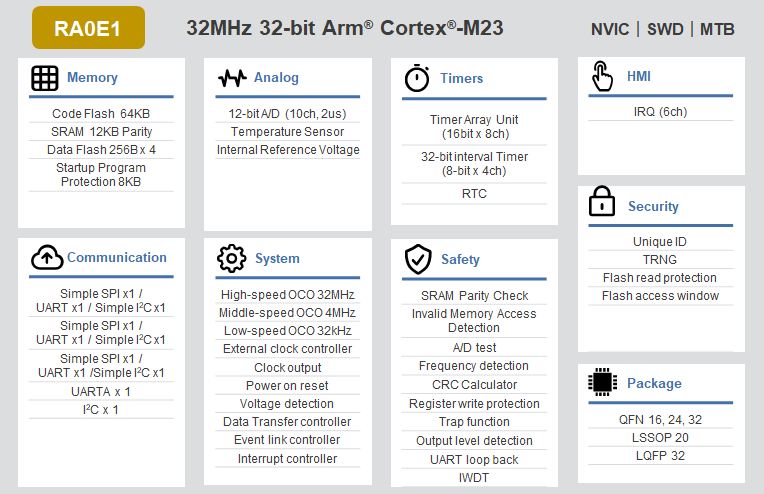
RA0E1 Features
-
32MHz Arm Cortex-M23 core
-
Up to 64KB Flash and 12KB SRAM
-
1KB data Flash (100,000 programming/erase (P/E) cycles)
-
16-pin and 32-pin package options
-
Wide voltage range from 1.6V to 5.5V
-
TAU (16-bit General PWM Timer)
-
TML32 (32-bit Interval Timer)
-
Real-time clock
-
12-bit Analog-to-Digital Converter
-
Temperature sensor
-
SAU (UART, Simple SPI, Simple I2C)
-
UART
-
I2C bus
-
Random number generator
-
Security features
-
+-1% high precision, high-speed on-chip oscillator
-
Flexible power architecture with fast wake-up capability
-
HAL driver code
-
Supports Arm ecosystem and Renesas original development tools
What I find most interesting about the R7FA0E1073CFJ chip are the following points:
-
The wide operating voltage of 1.6V~5.5V. In environments with strong interference, a 5V operating voltage can make the system more stable and reliable. When directly driving some MOSFETs, it can be driven directly from the IO port, which can help reduce costs.
-
The 12-BIT ADC can meet basic accuracy requirements in many application scenarios, such as temperature measurement and voltage detection, without the need for an external ADC, saving BOM costs as well as FLASH code.
Method Description
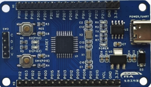
As this is my first time using Renesas MCU products, I accessed the Renesas RA MCU ecosystem community through the link provided by Jialichuang, downloaded the relevant materials for the development board, and installed the e2studio development environment.
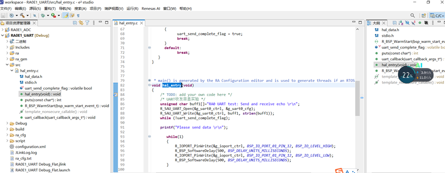
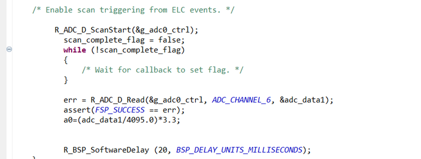
The purpose of this test is to collect external voltage using the internal 12-BIT ADC and send it to external devices via USART for observation.
System Block Diagram Introduction
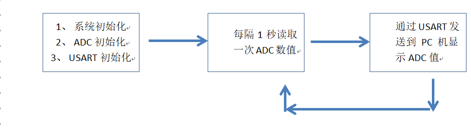
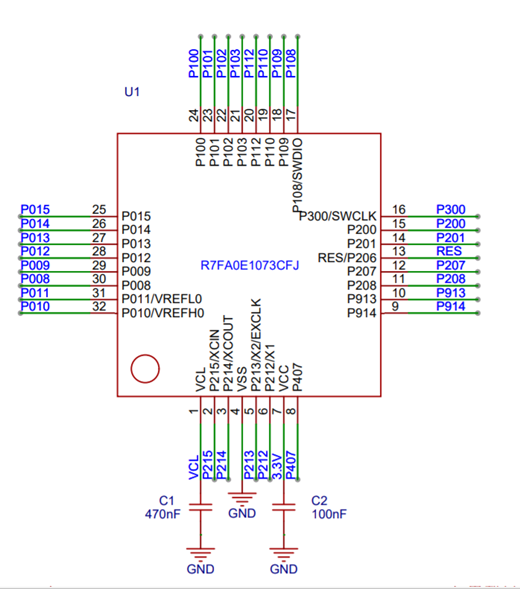
Code Introduction
Results & Conclusion
-
By comparing the values obtained from the ADC conversion of the stable DC voltage generated by the signal generator with the actual voltage values, the ADC acquisition accuracy meets the design requirements.
-
The R7FA0E1073CFJ chip is very easy for beginners to get started with and master. The development environment is user-friendly and easy to learn.

Need product and solution support
Please scan the code to register

Need technical support?
If you have any questions while using Renesas MCU/MPU products, you can scan the QR code below or copy the URL into your browser to enter the Renesas Technical Forum to find answers or get online technical support.

https://community-ja.renesas.com/zh/forums-groups/mcu-mpu/
1
END
1
Recommended Reading

Excellent Case Sharing from the Jialichuang Electric Competition: “Animated Clock”
Excellent Case Sharing from the Jialichuang Electric Competition: “Desktop Clock Design Based on Renesas”
Excellent Case Sharing from the Jialichuang Electric Competition: “Touch Control Light Strip Controller”
For more exciting content, please stay tuned.


Need product and solution support
Please scan the code to register