Walking on the waves, occasionally looking back, though there are no marks, I can still see the distant coast. It has been eight years since I graduated in 2015. I have worked in hardware for eight years, and my love for it has deepened. I still remember a friend I met in the student union during college; one day he suddenly recommended a microcontroller development board to me. At that time, I was in my sophomore year and had heard that microcontrollers would be a course starting next semester. I thought it was a fate arrangement and spent a fortune to buy Guo Tianxiang’s microcontroller development board. By some divine intervention, I was able to study until one or two in the morning during those loose college days! It was also because of a development board that I passed the computer level two exam twice (though I later realized it wasn’t very useful). I naturally got through it. The hardware knowledge that I didn’t understand before became clear. Later, I participated in many competitions organized by the school and at the national level, and I fell in love with hardware. At that time, I also became the professional representative of our class, but graduation always caught people off guard. After a busy period, I entered my current company. I remember I didn’t dare to write ‘hardware engineer’ on my resume and ended up writing ‘PCB engineer.’ Perhaps I was also doubtful about my hardware design abilities. At the beginning of my job, most of my time was spent familiarizing myself with the products, so I repaired the company’s old boards, looked at the schematics, and checked the materials, most of which required me to figure out on my own. Then came PCB design, learning Cadence software, and designing my first interface board. A year and a half flew by, and designing five or six-layer boards became quite easy. I remember once evaluating the PCB size and interface position corresponding to the product appearance. I had to learn the simplest SolidWorks operation. I also ventured into structural design. Later, when our structural design engineer left, I took on this job. Historically, hardware and structure have always been intertwined. The combination of PCB and structure produced a perfect product. Just like that, four years passed. As someone who works with hardware, I hadn’t even dealt with schematics; it was quite regrettable. Just when I was about to take it easy, my manager suddenly started giving me various schematic designs to teach me, and he was practically teaching me hands-on, but time only allowed me a month because he was leaving and wanted me to take over. It was a bittersweet feeling. The joy was a promotion and salary increase, but the sadness was that two projects came in at the same time. Schematics, PCB, structure… let’s start seriously with the schematics, as that’s all I could do. So I referred to the reference design, thinking that just deleting a few components would do the trick. However, when I started deleting capacitors, I got stuck, with questions flooding my mind: Why was this capacitor chosen for this capacity? Why is the voltage rating this? This capacitor’s material isn’t marked here? Why are there so many types of capacitors in this place? Forget it, let’s delete the resistors instead. Then more questions arose: What resistance value? What precision? What package size? Later, there were inductors… In the end, I kept everything as it was; since it worked, I left it unchanged. This ultimately led to BOM costs and larger board issues. I could do this the first time, and the second time too, but when the product was released, our pricing was quite high compared to similar products on the market. So my boss invited me to his office for tea. The message was simple: reduce BOM costs. The road ahead is long and winding.Below is the series of evaluations for the breadboard community’s Renesas RA6M4 MCU Evaluation Board evaluation activity, shared here for your reference.
1. Development Board Environment Setup
1.1. Hardware
Based on the CPK-RA6M4 evaluation board, it is equipped with Jlink, USB, and two PMOD interfaces. For interaction, there is one button and one LED, and for sensors, there is a potentiometer and a light sensor. Additionally, most IO interfaces have been brought out through pin headers. To perform DSP testing, a serial port needs to be connected to print debugging information via the serial port. (Note: The development board is designed with a 24M external crystal oscillator input, but it is not soldered, so when configuring the clock, make sure to switch to the internal clock).
1.2. FSP Software Configuration
The FSP software is the development configuration software. The first step is to configure the clock, as mentioned in 1.1. Since the external crystal oscillator is not soldered, the internal crystal oscillator needs to be used. The configuration is shown in Figure 1 below:
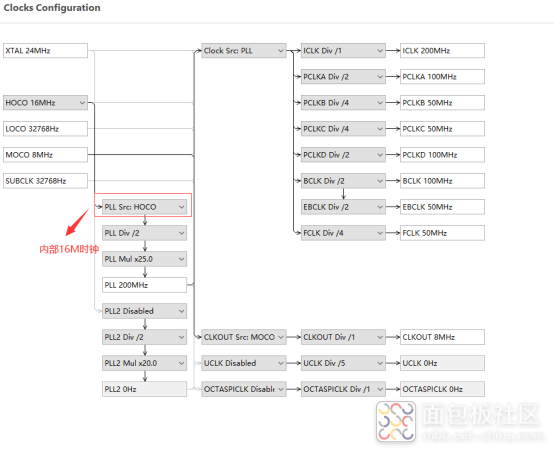
Figure 1 Clock Configuration
The second step is to configure the interface (LED). The LED is connected to port P106, and the P106 pin needs to be enabled. The configuration is shown in Figure 2 below: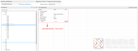 Figure 2 LED Pin ConfigurationThe third step is to configure the serial port. To facilitate debugging output, the serial port print function needs to be used, and the serial port configuration is shown in Figures 3a and 3b below:
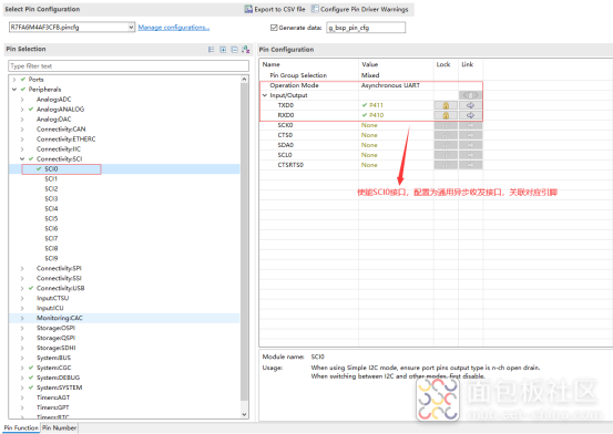 Figure 3a UART Configuration
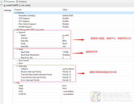 Figure 3b UART ConfigurationThe fourth step is to enable the DSP library, and the DSP library configuration is shown in Figure 4 below:
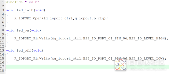
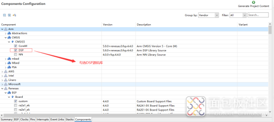 Figure 4 Configure DSP1.3. DriversThe drivers include LED and serial port driver programs: the LED driver program is shown below:
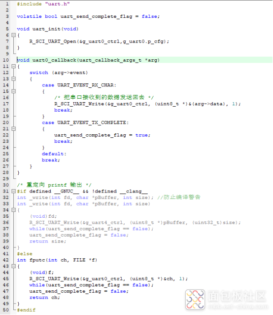
 The serial port driver is as follows:
 1.4. ApplicationA simple test for calculating the absolute value of array elements:
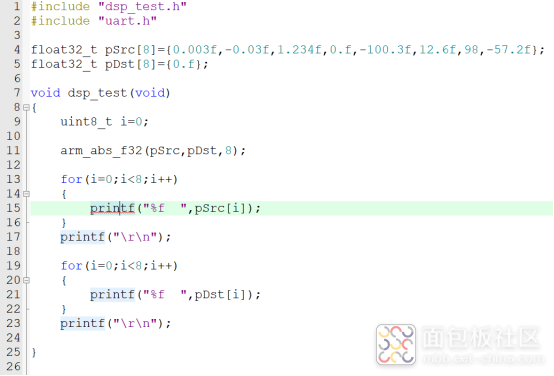 Test results: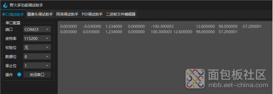
Figure 5 Result of Digital Signal Processing Absolute Value Calculation
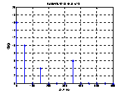
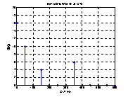
2. Fast Fourier Transform (FFT) Test2.1. Fast Fourier Transform The Fast Fourier Transform (FFT) is a general term for efficient and fast computation methods of the Discrete Fourier Transform (DFT) using computers, abbreviated as FFT. The FFT was proposed by J.W. Cooley and T.W. Tukey in 1965. By using this algorithm, the number of multiplications required for a computer to compute the DFT is greatly reduced, especially as the number of sampling points N increases, the savings in computation with the FFT algorithm becomes more significant. The example uses y=16+10sin(100πt)+4sin(300πt)+6sin(700πt) as the test sequence, with a sampling rate of 6400Hz, a fundamental frequency of 50Hz, and 128 sampling points. The DC component is 16, the fundamental component is 10, the third harmonic component is 4, and the seventh harmonic component is 6. The FFT outputs the amplitude of each harmonic and compares it with the harmonic amplitude of the sequence. 2.2. CMSIS-DSPThe CMSIS-DSP library is a rich collection of DSP functions optimized for various Arm Cortex-M processors (such as Cortex-M4, Cortex-M7, Cortex-M33, Cortex-M35, and Cortex-M55). The Arm Developer website contains more information and support resources regarding these processors.The CMSIS-DSP is widely used in the industry and can optimize C code generation through various third-party tools.The example routine uses the real FFT from the TransformFunctions in the DSP development package.Test program: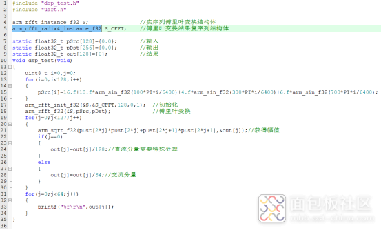 Serial output values, including DC components to the 63rd harmonic amplitude, are shown in Figure 6 below:
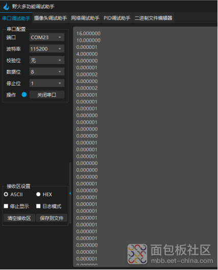 Figure 6 RA6M4 Microcontroller FFT Output ResultsTo conveniently visualize the data, the FFT results from the microcontroller are output via the serial port and imported into MATLAB for plotting. The results are compared with MATLAB’s transformation results, yielding the following results in Figure 7. It can be seen that the standard sine wave, when superimposed with the DC component, has values greater than 0; the standard sine wave, when superimposed with the third and seventh harmonics, shows distortion in the waveform. Comparing the RA6M4 transformation results with MATLAB’s transformation results, the amplitude at the corresponding frequency is the same, proving the correctness of the RA6M4’s FFT results.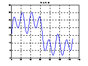
 It is important to note that the amplitudes of each frequency obtained after FFT processing based on ARM CMSIS DSP do not represent the true amplitude of the original signal at that frequency. To recover the original signal’s amplitude, the DC component needs to be divided by the FFT length, while other frequencies should be divided by half of the FFT length. In the test program, the FFT length is 128, so the DC amplitude is divided by 128, while the amplitudes of other frequencies are divided by 64..
END

Click to Read the Original Text and Apply for Free