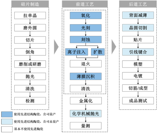
Precision ceramic components are key parts of core equipment in several critical processes of semiconductor manufacturing, such as lithography, etching, thin film deposition, ion implantation, and CMP, including bearings, guide rails, liners, electrostatic chucks, and mechanical handling arms. They play supporting, protective, and guiding roles, especially within the equipment chambers.
Usage of Advanced Ceramics in Semiconductor Manufacturing
Image Source: Kema Technology
This article systematically summarizes the application of precision ceramic components in major semiconductor equipment.

Front-End Processes: Precision Ceramics in Wafer Manufacturing Equipment
01 Lithography Machines
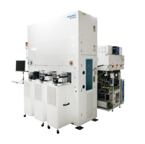
In high-end lithography machines, to achieve high process precision, ceramic components with good functional complexity, structural stability, thermal stability, and dimensional accuracy are widely used, such as electrostatic chucks, vacuum chucks, blocks, magnetic steel frame water-cooled plates, mirrors, guide rails, workpiece tables, and mask tables.Representative ceramic components include electrostatic chucks and mobile platforms.
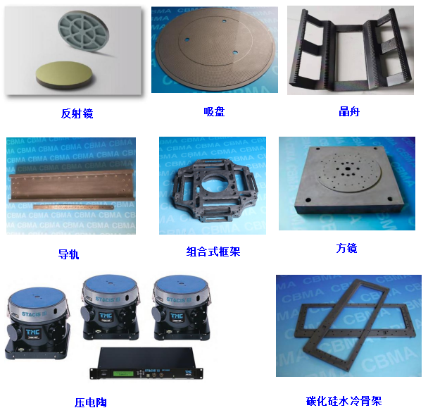
Representative Ceramic Components: Electrostatic Chucks, Mobile Platforms.
-
Electrostatic Chucks
Electrostatic chucks are widely used tools for holding and transferring wafers in semiconductor component manufacturing, extensively used in plasma and vacuum-based semiconductor processes such as etching, chemical vapor deposition, and ion implantation.
-
Major Ceramic Materials
Alumina ceramics, silicon nitride ceramics
-
Manufacturing Challenges
Complex structural design, material selection and sintering, temperature control, high-precision processing technology
-
Mobile Platforms
The material system design of the lithography machine’s mobile platform is key to achieving high precision and high speed. To effectively resist deformation caused by high-speed movement during scanning, the platform material should include low thermal expansion materials with high specific stiffness, meaning these materials should have high modulus while also meeting low density requirements. Additionally, the material needs to have high specific stiffness, allowing the entire platform to maintain the same level of distortion while withstanding higher acceleration and speed. By increasing throughput without increasing distortion while switching masks at higher speeds, work efficiency is improved while ensuring high precision.
-
Major Ceramic Materials
Cordierite ceramics, silicon carbide ceramics.
02 Etching Machines
To transfer the chip circuit pattern from the mask to the wafer to achieve the desired chip functionality, the etching process is a crucial step. The ceramic components used in etching equipment mainly includechambers, viewports, gas dispersion plates, nozzles, insulating rings, covers, focus rings, and electrostatic chucks.
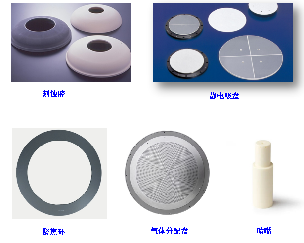
Representative Ceramic Components: Electrostatic Chucks, Focus Rings, Gas Distribution Plates.
-
Chambers
As the minimum feature size of semiconductor devices continues to shrink, the requirements for wafer defects become stricter. To avoid contamination from metal impurities and particles, stricter requirements have been placed on the materials of semiconductor equipment chambers and their internal components. Currently, ceramic materials have become the primary material for etching machine chambers.
-
Material Requirements
(1) High purity, low metal impurity content;
(2) The main components must have stable chemical properties, especially low reaction rates with halogen corrosive gases;
(3) High density, few open pores;
(4) Fine grains, low grain boundary phase content;
(5) Excellent mechanical properties, easy to process;
(6) Some components may have additional performance requirements, such as good dielectric properties, conductivity, or thermal conductivity.
-
Major Materials
Quartz, silicon carbide, aluminum nitride, alumina, silicon nitride, yttrium oxide, etc.
-
Gas Distribution Plates
Its surface is densely covered with hundreds to thousands of tiny holes, like a precisely woven neural network, capable of accurately controlling gas flow and injection angles, ensuring that every inch of the wafer processing is evenly “bathed” in process gases, improving production efficiency and product quality.
-
Technical Challenges
Gas distribution plates not only have extremely high requirements for cleanliness and corrosion resistance but also have strict requirements for the consistency of the small hole diameters and burrs on the inner walls of the holes. If the diameter size tolerance and consistency standard deviation are too large or if there are any burrs on the inner walls, it will lead to uneven deposition film thickness, directly affecting the process yield of the equipment.
-
Major Ceramic Materials
CVD-SiC, alumina ceramics, silicon nitride ceramics, etc.
-
Focus Rings
The function of the focus ring is to provide balanced plasma, requiring similar electrical conductivity to silicon wafers. Previously used materials were mainly conductive silicon, but fluorine-containing plasmas react with silicon to produce volatile silicon fluoride, greatly shortening its service life, leading to frequent component replacements and reduced production efficiency. SiC has similar electrical conductivity to single crystal Si and better resistance to plasma etching, making it a suitable material for focus rings.
-
Major Ceramic Materials
Silicon carbide ceramics
03 Thin Film Deposition Equipment
In PVD, CVD, and other thin film deposition process equipment, ceramic electrostatic chucks are also core components. Additionally, gas distribution plates, ceramic heaters, and chambers also use ceramic components.
Ceramic Heaters
Representative Components: Electrostatic Chucks, Ceramic Heaters.
-
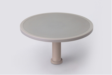
Ceramic Heaters
Ceramic heaters are directly applied in process chambers, in contact with wafers, not only supporting the wafers but also ensuring that the wafers achieve stable and uniform process temperatures, making them key components in semiconductor thin film deposition equipment.
-
Major Ceramic Materials
Aluminum nitride ceramics, alumina ceramics.
 Back-End Processes: Precision Ceramics in Packaging and Testing Equipment
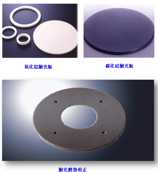
01 Chemical Mechanical Polishing (CMP) Equipment
In CMP equipment,polishing plates, handling arms, correction platforms, vacuum chucksare all made of ceramic materials.
02 Wafer Cutting and Packaging Equipment
-
Core Components
-
Cutting Blades
Diamond-ceramic composite materials, cutting speed up to 300mm/s, edge chipping < 1μm.
-
Hot Press Welding Heads
Aluminum nitride ceramics, thermal conductivity 220 W/mK, ensuring uniformity of solder joint temperature ±2℃ for packaging substrates.
-
Low-Temperature Co-fired Ceramics (LTCC)
Wiring accuracy up to 10μm, supporting 5G millimeter-wave transmission.
-
Ceramic Splitting Knives
Important tools in the wire bonding process. Commonly used alumina ceramics, zirconia-reinforced alumina ceramics, etc.
Ceramic Splitting Knives
03 Testing Probe Stations
-
Core Components
-
Ceramic Adapter Substrates
Beryllium oxide ceramics, aluminum nitride ceramics
-
High-Frequency Testing Fixtures
Aluminum nitride ceramics
 Support Systems: Ceramic Parts in Wafer Transport and Clean Environments
01 Wafer Transport Robots
-
Core Components
-
Mechanical Arms
Alumina ceramics, silicon carbide ceramics.
-
Mechanical Arm Joint Bearings
Zirconia ceramic balls, friction coefficient < 0.001, lifespan > 10 million cycles in vacuum.
-
Mechanical Hand Fingers
Silicon carbide ceramics, resistant to 150℃ baking, particle release < 0.1 per cm2.
02 Ultra-Pure Water and Gas Delivery Systems
-
Core Components
-
Valve Seals
Silicon nitride ceramics, resistant to hydrofluoric acid corrosion.
-
Pipe Linings
High-density alumina ceramics.
References: China Powder Network, Kema Technology Prospectus, and Feng Technology
Note: Images are for non-commercial use; please notify for removal if there are copyright issues! To join the powder industry group chat, please add the editorial department WeChat: 18553902686