Follow+Star PublicAccount, don’t miss exciting content

Source | nhczp
Editor | strongerHuang
Everyone should be using USB drives, and the storage chip in the USB drive is NandFlash. The 64G USB drive you bought actually does not have 64G, one reason is the existence of bad blocks.
Due to manufacturing processes and other reasons, it cannot be guaranteed that NandFlash is free of bad blocks, so it is necessary to “select out the bad blocks”.
This article will explain the ECC verification principle and implementation used for NandFlash.
Introduction to ECC
Since the manufacturing process of NAND Flash cannot guarantee that the NAND Memory Array maintains reliable performance throughout its lifecycle, bad blocks will occur during the production and usage of NAND.To ensure data reliability, systems using NAND Flash generally adopt certain bad block management strategies, and the premise of managing bad blocks is to reliably detect them.
If there are no issues with operation timing and circuit stability, when errors occur in NAND Flash, it generally does not cause the entire Block or Page to be unreadable or completely erroneous; rather, only one or a few bits in the entire Page (for example, 512 Bytes) are erroneous.Common methods for data verification include parity checks, CRC checks, etc., while in NAND Flash processing, a more specialized verification method is generally used—ECC. ECC can correct single-bit errors and detect double-bit errors, and the calculation speed is very fast, but it cannot correct errors of more than 1 bit and does not guarantee detection of errors of more than 2 bits.
Principle of ECC
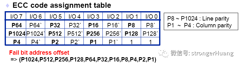
Generally, ECC generates 3 bytes of ECC check data for every 256 bytes of raw data. These three bytes consist of 24 bits divided into two parts: 6 bits of column parity and 16 bits of row parity, with the two excess bits set to 1, as shown in the figure below:
The generation rules for the column parity of ECC are shown in the figure below:
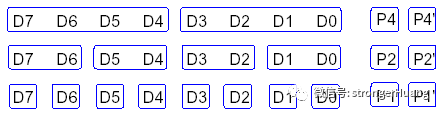
Expressed in mathematical notation as:
P4=D7(+)D6(+)D5(+)D4
P4`=D3(+)D2(+)D1(+)D0
P2=D7(+)D6(+)D3(+)D2
P2`=D5(+)D4(+)D1(+)D0
P1=D7(+)D5(+)D3(+)D1
P1`=D6(+)D4(+)D2(+)D0
Note: Here (+) denotes the