In the visual perception systems of autonomous driving, the massive image data captured by sensors must be transmitted to processors for processing. This process not only generates redundant data but also causes delays, which may affect decision-making in emergencies. Similarly, in the field of security monitoring, real-time image classification faces bottlenecks in data transmission and processing efficiency. Now, a team from the University of British Columbia in Canada has published research in Optics Express proposing a solution based on silicon photonic integration technology called ‘In-Sensor Imaging Classification’, bringing new hope to solve these issues.
In traditional image classification schemes, the sensor and computing unit are separate, and visible light signals must undergo a multi-step conversion of ‘optical-electrical-optical’ before being processed by the photon neural network. This not only complicates the process but also causes data redundancy and latency. The new scheme cleverly integrates sensing and computing, utilizing an array of pn-doped micro-ring resonators to directly convert visible light signals in free space into near-infrared light signals transmitted in silicon waveguides, which are then processed by the photon neural network, eliminating unnecessary conversion steps and fundamentally simplifying the architecture.
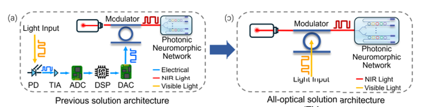
Figure 1: All-optical modulation concept: Schematic diagram of processing steps for single-channel image classification, using a neuromorphic computing system to implement traditional solutions (a) and all-optical solutions (b)
The core innovation of this scheme lies in the all-optical modulator, which is based on pn-doped micro-ring resonators, achieving ‘light-controlled light’ through thermal-optical effects and plasma dispersion effects. When visible light illuminates the silicon micro-ring, on one hand, electrons transition from the valence band to the conduction band, generating free carriers, which cause the micro-ring resonance wavelength to blue-shift due to the free carrier dispersion effect; on the other hand, electron-hole pairs recombine to produce heat, and the thermal-optical effect causes the resonance wavelength to red-shift. The combined effects determine the final shift of the resonance wavelength, laying the foundation for precise modulation.
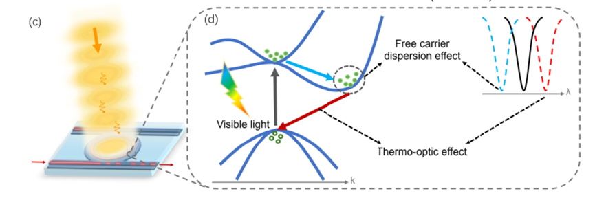
Figure 2 (c): Schematic diagram of all-optical modulation principle: The output near-infrared signal corresponds to the input visible light signal, and the visible light entering from the top of the ring resonator can modulate the intensity of the near-infrared light. (d) Schematic diagram of the working mechanism of the all-optical modulation method: The absorbed visible light excites electrons from the valence band to the conduction band in silicon. Next, the band-to-band transitions corresponding to the free carrier dispersion effect lead to a blue shift of the micro-ring resonance wavelength; the indirect electron-hole recombination corresponding to the thermal-optical effect results in a red shift of the micro-ring resonance wavelength.
Even more astonishingly, the team has also achieved ‘modulation state switching’. By controlling the open and short-circuit states of the pn junction, the dominant relationship between the two effects can be adjusted. In the short-circuit state, free carriers migrate quickly, eliminating the free carrier dispersion effect, enhancing the thermal-optical effect, and ultimately achieving a maximum modulation depth of 16.96 dB, which provides strong support for subsequent efficient computing.
In terms of chip structure design, the scheme is highly ingenious. First is the micro-ring resonator array, composed of N parallel-coupled micro-rings doped with pn, each micro-ring can independently modulate different channel signals, encoding visible light image signals into multi-channel near-infrared light signals. Subsequently, these modulated near-infrared light signals are directed to an M×N weight library to complete matrix multiplication, and finally detected by balanced photodetectors to achieve weighted summation, all efficiently completed on-chip without the need for complex external conversions.
To verify the feasibility of the scheme, the team tested the MNIST handwritten digit dataset. By training a multilayer perceptron model and utilizing the dot product operation achieved by the micro-ring array (with an effective resolution of nearly 8 bits, meeting data processing requirements), the final imaging classification accuracy reached 96.82%, comparable to the accuracy of traditional schemes, but with significant performance advantages. In terms of energy consumption, a single classification task with an 8×8 pixel input only requires 54.28 μJ, far lower than the CMOS sensor + photon computing (66.8 μJ) and CMOS sensor + electrical computing (200.06 μJ) architectures; if non-volatile materials are integrated, the energy consumption for a 28×28 pixel input can be reduced to 16.55 μJ. In terms of latency, due to the reliance on thermal-optical effects, it is 20 times faster than traditional ‘electrical-optical hybrid’ architectures, showing significant advantages in scenarios with high real-time requirements such as autonomous driving.
This research not only achieves a technological breakthrough but also promotes the practical application of photon computing. In the future, with the further development of silicon photonic integration technology, this scheme is expected to be widely applied in fields such as autonomous driving, security monitoring, and drone vision, allowing devices to ‘see faster and compute more efficiently’.
This article is for learning and communication purposes only. Please point out any errors in the text, and contact us for removal if there is any infringement.
Original link: https://doi.org/10.1364/OE.567917