|
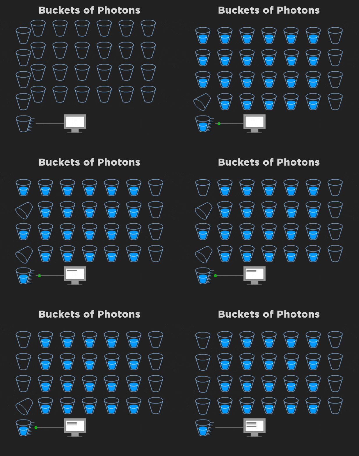
Based on semiconductor technology, CCD image sensors have changed the history of recording images with film. Today, digital imaging is not only an important tool for scientific analysis but has also penetrated into everyone’s daily life.
|

Willard S. Boyle (left) and George E. Smith (right) invented CCD technology in 1969.
In 2009, Willard S. Boyle and George E. Smith were awarded the Nobel Prize in Physics for their invention of the CCD (Charge-coupled Device).
Joseph Nordgren, chairman of the Nobel Prize Committee, stated at the award announcement press conference: “The way society records images today is entirely based on the research of CCD. The practical significance of this research is enormous… it has changed our lives, not only in the scientific field but across society as a whole.”
Before the invention of the digital camera in 1975, people recorded images using film. The process can be summarized as follows: light passes through the camera lens, and the shutter speed determines the amount of exposure. Light causes a chemical reaction in the silver salts on the film, ultimately creating a latent image on the film. The image is then developed in a darkroom to form a negative, which is finally printed using the negative.
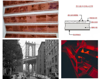
Film photography requires complex processing to obtain images.
[Image source from the internet]
In October 1969, Smith and Boyle had a lunch discussion at Bell Labs that sparked inspiration. After lunch, they continued to explore the idea and conceived the ubiquitous imaging invention of CCD that very day. However, the journey from creating a prototype to developing a practical technology usable by scientists and photographers was long and arduous. Although CCD later dominated the field of astronomy, its initial resolution was very low, rendering it practically useless. At that time, the signal-to-noise ratio of CCD was poor, making it difficult to predict its bright future.
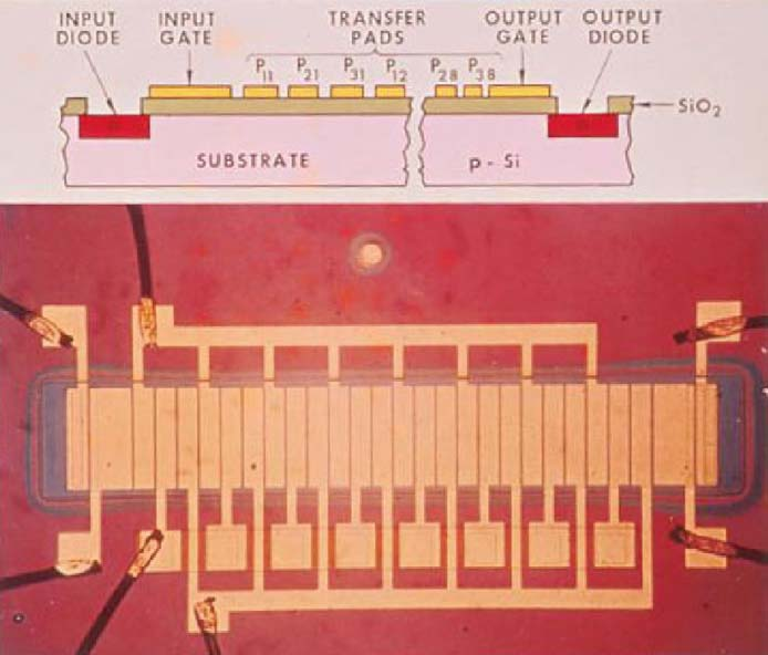
The first CCD device.
Source: Literature [4]
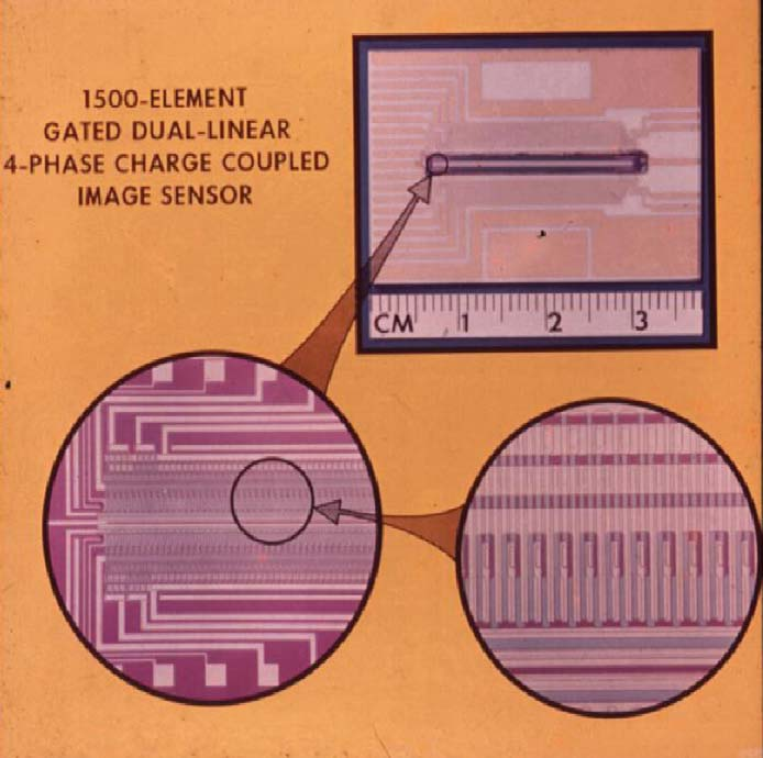
The first CCD integrated device.
Source: Literature [4]
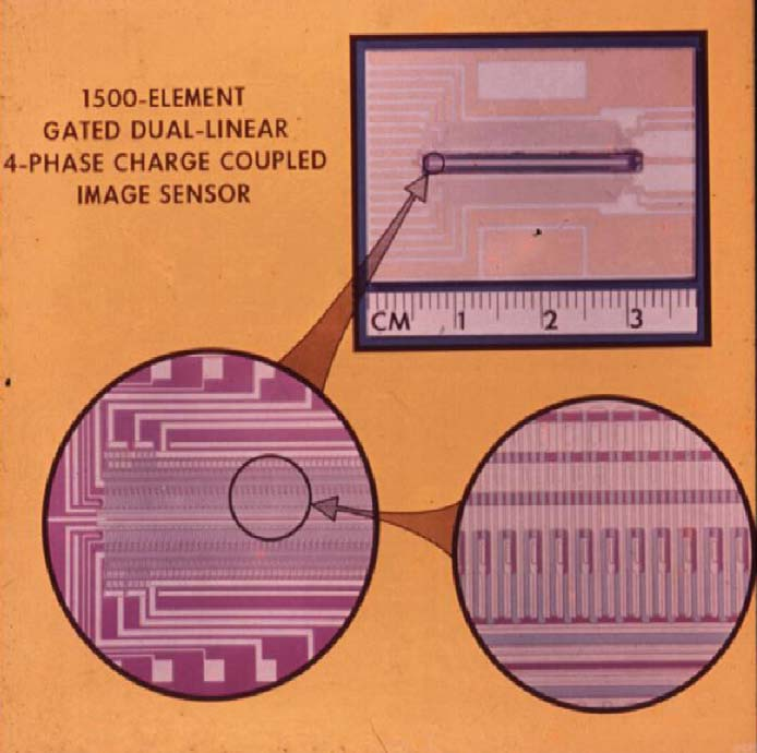
Early linear imaging CCD.
In the following time, hundreds of scientists and engineers worked hard to gradually push CCD towards practicality. Companies such as Fairchild, Tektronix, and Texas Instruments from the United States, as well as Sharp, Sony, Toshiba, and NEC from Japan, all made significant contributions. Applications in aerospace, science, and consumer electronics benefited from funding invested through various channels to solve CCD problems, but the challenges remained tough, marking a very arduous development path.
CCD is a type of semiconductor device capable of converting optical images into digital signals. The tiny photosensitive material implanted on the CCD is called a pixel. The higher the number of pixels and the larger the area, the higher and clearer the imaging quality. The CCD has many orderly arranged capacitors that can sense light, store signals, and convert images into digital signals. Controlled by external circuits, each small capacitor can transfer its charge to the adjacent image processor to form an image.
MOS capacitors are the most basic unit that constitutes CCD, being the simplest structure in metal-oxide-semiconductor (MOS) devices.
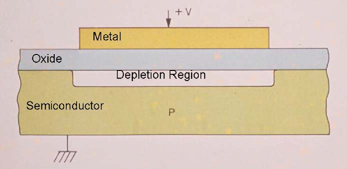
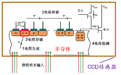
The basic working process of CCD mainly involves the generation, storage, transfer, and detection of signal charges:
(1) Injection (Generation) of Signal Charge: In CCD, the method of charge injection can be divided into two categories: optical injection and electrical injection. When light strikes the CCD silicon chip, electron-hole pairs are generated within the semiconductor near the gate. Most carriers are repelled by the gate voltage, while a small number of carriers are collected in the potential well to form signal charges.
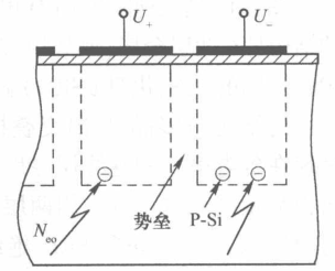
Back-illuminated optical injection.
Electrical injection refers to the process where CCD samples the signal voltage or current through its input structure and then converts the signal voltage or current into signal charge injected into the corresponding potential well. Common methods of electrical injection include current injection and voltage injection.
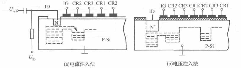
Electrical injection method.
Source: Literature [8]
(2) Storage of Signal Charge: The second step in the CCD working process is the collection of signal charge, which is the process of collecting the charges excited by incident photons to form signal charge packets.
When a positive bias is applied to the electrode on the SiO2 surface, a depletion region (potential well) is formed in the P-type silicon substrate, and the depth of the depletion region increases with the applied positive bias. The minority carriers (electrons) are absorbed into the region under the highest positive bias electrode, forming a charge packet (potential well). For N-type silicon substrate CCD devices, the minority carriers are holes when positive bias is applied.
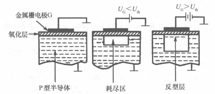
Charge storage.
Source: Literature [8]
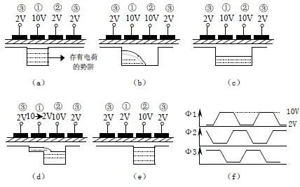
(3) Transfer (Coupling) of Signal Charge: The third step in the CCD working process is the transfer of signal charge packets, which is the process of transferring the collected charge packets from one pixel to the next until all charge packets are outputted.
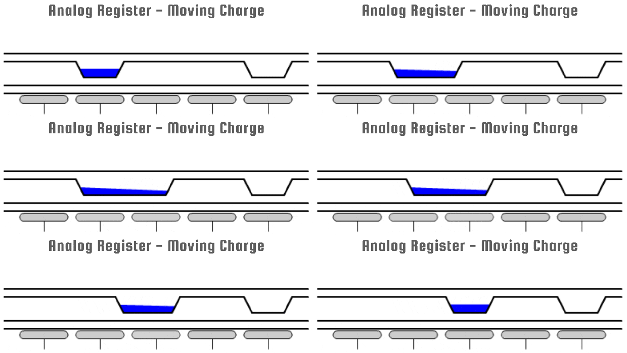
Charge transfer.
Source: Literature [7]
Charge transfer method in three-phase CCD.
(a) Initial state; (b) Charge transfers from electrode ① to electrode ②; (c) Charge is evenly distributed under electrodes ① and ②; (d) Charge continues to transfer from electrode ① to electrode ②; (e) Charge is fully transferred to electrode ②; (f) Three-phase overlapping pulse.
Source: Literature [8]
(4) Detection of Signal Charge: The fourth step in the CCD working process is the detection of charge, which is the process of converting the charge transferred to the output stage into current or voltage.
The main types of charge output are: 1) current output; 2) floating gate amplifier output; 3) floating diffusion amplifier output.
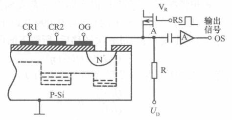
Charge detection circuit.
Source: Literature [8]
Diagram of CCD working process.
Source: Literature [6]
The CCD image sensor is an array composed of MOS (metal-oxide-semiconductor) capacitors arranged in a specific pattern. A very thin layer (about 120nm) of silicon dioxide is grown on a P-type or N-type silicon substrate, followed by the sequential deposition of metal or doped polysilicon electrodes (gates) on the silicon dioxide layer, forming a regular array of MOS capacitors, combined with input and output diodes at both ends to create the CCD chip.
According to the different arrangements of pixels, CCDs can be divided into linear arrays and area arrays.
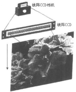
Linear array CCDs scan one line at a time, and to obtain a two-dimensional image video signal, a scanning method must be employed. Linear array CCDs are further divided into single-channel linear array CCDs and dual-channel linear array CCDs.
Single-channel linear array CCD: many transfer cycles, low efficiency. Suitable only for imaging devices with fewer pixel units.
Dual-channel linear array CCD: transfer cycles are reduced by half, and its total transfer efficiency is doubled.
Linear array CCD.
Source: Literature [6]
Area array CCD: By arranging the one-dimensional linear array CCD’s photosensitive units and shift registers in a two-dimensional array, a two-dimensional area array CCD can be constructed. The area array CCD exposes the entire image simultaneously.
Frame transfer area array CCD—Advantages: simple electrode structure, small photosensitive area. Disadvantages: requires a large storage area.
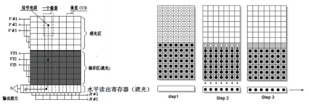 Frame transfer area array CCD structure and working process.
Source: Literature [6]
Interline transfer area array CCD—Advantages: significantly improved transfer efficiency. Disadvantages: more complex structure.
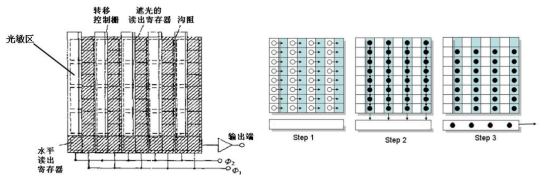
Interline transfer area array CCD structure and working process.
Source: Literature [6]
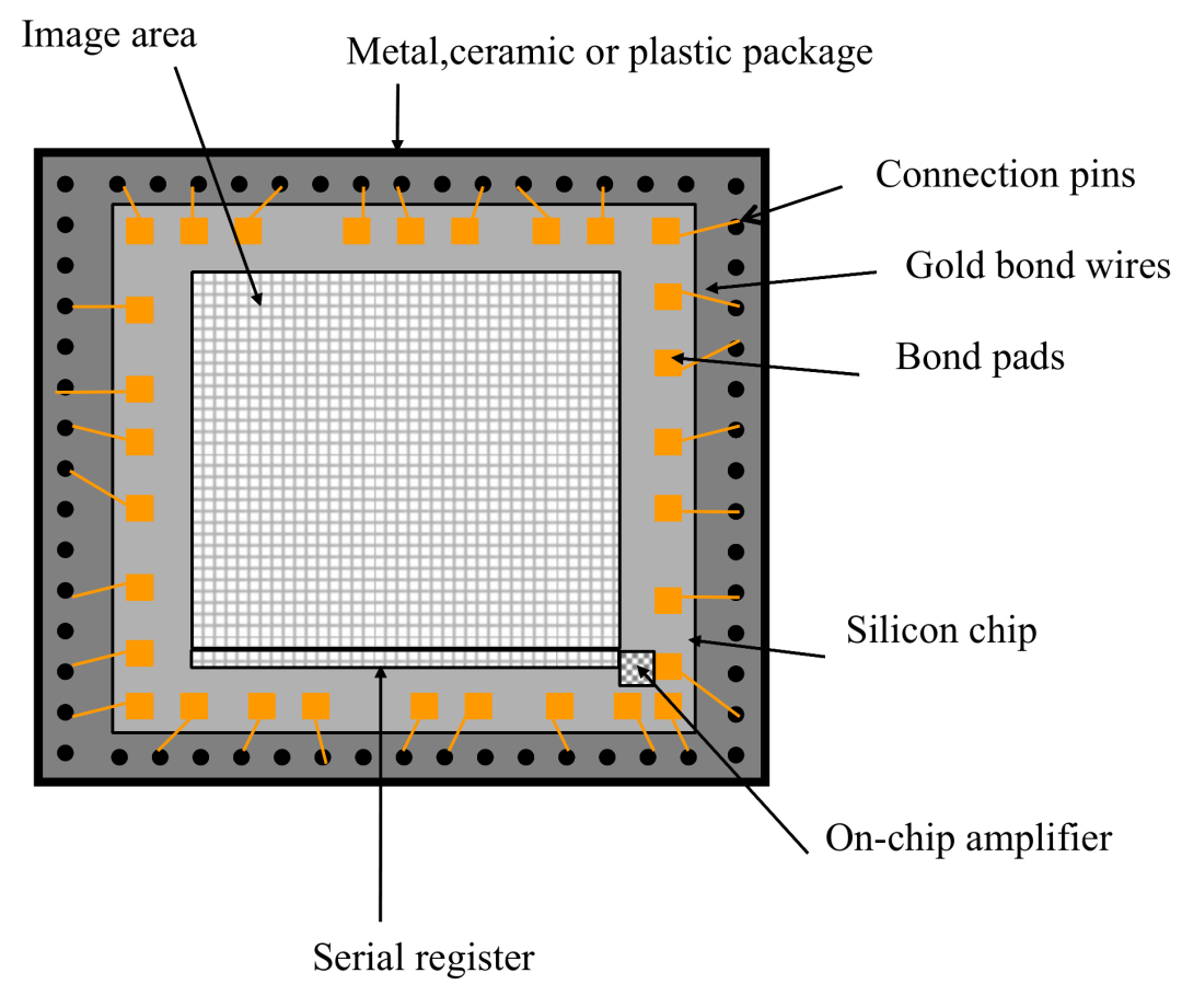
CCD chip structure.
Image source from the internet.
The invention of CCD is epoch-making; its emergence has greatly expanded and extended the human ability to capture information with the eyes, which accounts for 85% of this important organ.
Three main factors have promoted the rapid development of CCD: First, CCDs are small in size, light in weight, low in power consumption, ultra-low noise, have a large dynamic range, good linearity, and are reliable and durable. Second, this device can compete with vacuum tubes in terms of shape, speed, appearance quality, and cost. Third, new detectors are needed for space imaging applications.
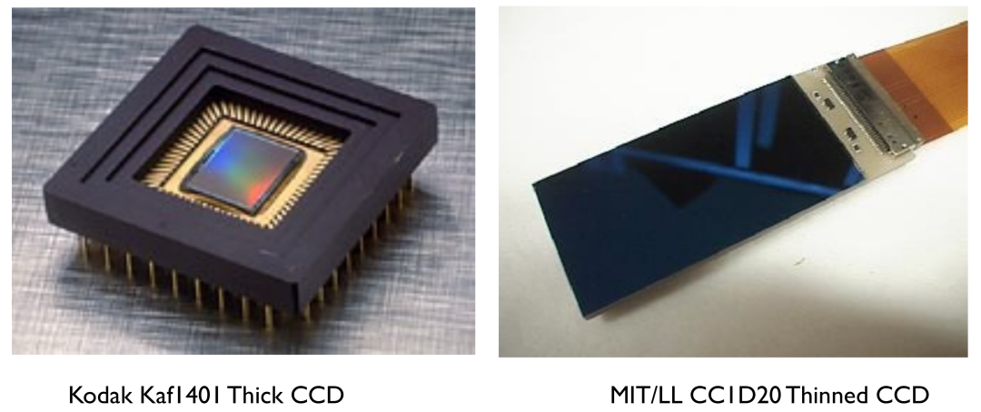
In the 1970s, Bell Labs in the United States successfully developed the world’s first CCD, whose birth marked a leap in imaging and video technology. In 1973, Fairchild Company applied CCD technology in the commercial field, producing the first commercial CCD imaging device, opening the path for CCD in the industrial sector. By the late 1980s, CCD had replaced electronic tubes in most video applications. In the 1990s, CCD was applied in resolution imaging, widely used in professional electronic photography, space exploration, X-ray imaging, and other scientific fields.
Two types of CCD products.
Image source from the internet.
The results of market applications demonstrate that CCD is a significant technological revolution in the scientific field. After being overlooked for decades, it rightfully received the Nobel Prize in 2009.
Continuous Transformation
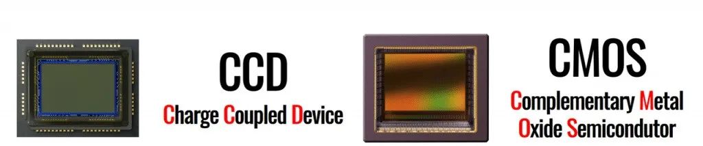
However, scientific and technological progress has never stopped. In 1998, the CMOS image sensor (Complementary Metal-Oxide-Semiconductor Image Sensor) was born. The photoelectric information conversion function of CMOS is similar to that of CCD, with the distinction being the different methods of transmitting the information after photoelectric conversion. CMOS features simple information reading methods, fast output rates, low power consumption (about 1/10 of CCD chips), small size, light weight, high integration, and low cost. Since 2008, major manufacturers have gradually started using back-illuminated CMOS in various digital camera products. Since then, CMOS image sensors have developed rapidly.
CMOS replaces CCD.
Image source from the internet.
As technology continues to develop, we believe that one day more types of sensors will emerge; it is only a matter of time. When we look back at the past, reflecting on the eras of film, CCD, and CMOS, we will undoubtedly marvel at the rapid advancements of technology.
-
https://www.nobelprize.org/prizes/physics/2009/summary/
-
Zhang Rujing. The Story Behind the Semiconductor Industry [M]. Tsinghua University Press, 2013.
-
Dong Yiting. Research on the Development of Photography Technology and Its Role in Contemporary Society [D]. Harbin Normal University, 2016.
-
Smith, G. E. (2009). “The invention and early history of the CCD.” Nuclear Instruments and Methods in Physics Research Section A: Accelerators, Spectrometers, Detectors and Associated Equipment 607(1): 1-6.
-
https://www.microscopyu.com/digital-imaging/introduction-to-charge-coupled-devices-ccds
-
https://www.mega-9.com/tech/tech-45.html
-
https://specinstcameras.com/what-is-a-ccd/
-
Wang Qingyou. Application Technology of Image Sensors [M]. Electronics Industry Press, 2019.
-
https://www.docin.com/p-505990925.html
-
http://dc.yesky.com/88/31913588all.shtml
Reproduced content only represents the author’s views.
It does not represent the position of the Institute of Physics, Chinese Academy of Sciences.
Source: Institute of Semiconductors, Chinese Academy of Sciences

Editor: Lychee Jelly
Recent Hot Articles Top 10
↓ Click the title to view ↓
1. After watching “The Beginning”, I discovered the secrets of the protagonist’s loop.
2. Will urinating on high-voltage power lines electrocute you? | No.290
3. Cao Zexian: From Quadratic Equations to Gauge Field Theory.
4. Why did this year’s New Year’s Eve suddenly disappear?
5. Would you dare to drink the “milk” produced by cockroaches?
6. Will the Tonga volcano eruption that caused the entire region to lose contact affect China?
7. If the universe began with the Big Bang, what caused the Big Bang?
8. How did Michael Jackson lean forward at 45 degrees?
9. Asleep but not asleep? Edison teaches you the skill of learning while sleeping.
10. Groundhogs: Stop, don’t hit anymore!
Click here to view all past hot articles.