
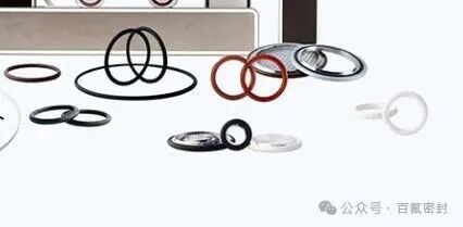
Introduction: In the nanometer battlefield of semiconductor manufacturing, any material defect can trigger a “butterfly effect”—a 0.1μm particle contamination is enough to scrap an entire wafer; a microsecond sealing failure can lead to millions of dollars in equipment downtime. Perfluoroether rubber (FFKM), with its “zero-compromise” performance in extreme environments, has become an irreplaceable sealing core in advanced processes, from 7nm to 3nm, from etching chambers to EUV lithography machines, acting as an “invisible guardian” to ensure precision and stability at every step of the process.
The Ultimate Test in Semiconductor Manufacturing: Why Only Perfluoroether Can Pass?
The requirements for sealing materials in semiconductor manufacturing have surpassed traditional industrial boundaries, forming three critical “life-or-death” standards, and perfluoroether rubber is the only elastomeric material that meets all these standards.
1. Corrosion Resistance: Maintaining Molecular Stability in a “Chemical Storm”
The media used in etching and ion implantation processes can be described as a “material corrosion laboratory”:
– The NF₃ (nitrogen trifluoride) plasma in dry etching can generate fluorine radicals with energy up to 480kJ/mol, easily breaking most chemical bonds;
– The BOE solution (a mixture of HF and NH₄F) used in wet cleaning has a corrosion rate on rubber that is more than ten times that of ordinary industrial acids.
Data from a leading wafer manufacturer shows:
– In 80℃, 40% concentration HF solution, perfluoroether rubber soaked for 2000 hours showed a volume change rate of only 0.7%, with a tensile strength retention of 97%, and no corrosion marks on the surface;
– Other elastomers (including high-performance fluororubber) showed swelling and cracking within 300 hours under the same conditions, with a volume change rate exceeding 20%, completely losing sealing capability.
The absolute advantage at the molecular level: The molecular chains of perfluoroether rubber are composed of carbon-fluorine bonds (bond energy 485kJ/mol), and contain no hydrogen atoms, unsaturated bonds, or polar groups, fundamentally eliminating the attack targets for fluorine radicals. This “perfluoro barrier” allows it to withstand almost all known semiconductor process media, including ClF₃ (chlorine trifluoride), known as a “chemical weapon.”
2. Ultra-Clean Performance: From “Zero Exudation” to “Zero Particles”
Advanced processes have entered the realm of “atomic-level control” for cleanliness:
– The SEMI F57 standard specifies that for sealing materials in processes of 7nm and below, the exudation of metal ions (Na⁺, K⁺, Fe³⁺, etc.) must be ≤1ppb (parts per trillion);
– In vacuum chambers, the material’s total mass loss (TML) must be ≤0.005% to avoid forming molecular-level contaminants on the wafer surface.
Measured data for perfluoroether rubber (after electronic-grade purification):
– Total metal ion exudation: <0.5ppb (below detection limit), far below the 1ppb threshold required for EUV lithography;
– After 24 hours of vacuum baking at 120℃, TML (total mass loss) = 0.003%, CVCM (condensable volatile matter) = 0.001%, fully meeting ultra-high vacuum environment requirements.
Process support: Perfluoroether rubber uses a “no-additive” formulation system, employing supercritical CO₂ extraction technology to remove residual oligomers, with surface roughness controlled below Ra0.05μm, eliminating particle shedding from the source—this is why perfluoroether is the only recognized elastomeric sealing material in the optical chambers of EUV lithography machines.
3. Stability Under Extreme Conditions: Maintaining Sealing Precision in “Ice and Fire Alternation”
The dynamic conditions of semiconductor manufacturing pose extreme challenges to the physical properties of materials:
– Deposition chambers (CVD/PVD) require rapid switching between 300℃ high temperatures and room temperature (heating rate 5℃/min), cycling 40 times a day, which can cause ordinary materials’ molecular chains to break;
– The pressure in etching machines frequently alternates between 10⁻⁷Pa (ultra-high vacuum) and atmospheric pressure, requiring seals to withstand repeated “negative pressure-positive pressure” loads, where any loss of elasticity can lead to leakage.
Durability test results for perfluoroether rubber:
– After 5000 cycles of thermal shock from 300℃ to room temperature, the compression set remains ≤6% (industry standard requires ≤20%), with no change in sealing surface fit;
– After alternating between 10⁻⁷Pa vacuum and atmospheric pressure for 100,000 times, the leakage rate remains stable at 1×10⁻¹⁰ Pa·m³/s (first-class vacuum sealing standard is 1×10⁻⁹ Pa·m³/s).
Performance roots: The glass transition temperature (Tg) of perfluoroether rubber is as low as -40℃, maintaining high elasticity at low temperatures; its highly cross-linked molecular structure (cross-link density is 2-3 times that of ordinary elastomers) prevents plastic flow under high temperature and pressure, fundamentally solving the chain reaction of “thermal aging-sealing failure.”
Case Studies: The Irreplaceability of Perfluoroether in Advanced Processes
Case 1: TSMC’s “Zero-Failure” Sealing Solution for 3nm Etching Machines
In the etching process of the 3nm FinFET process, the chamber uses NF₃/Ar mixed plasma (power 1000W) at a temperature of 280℃, where various sealing materials previously attempted showed rapid failure:
– High-performance fluororubber showed a fluorine crystallization layer on the surface after 500 hours of operation (EDS analysis showed fluorine content reached 40%), with a leakage rate rising to 2×10⁻⁸ Pa·m³/s, triggering equipment alarms;
– After switching to perfluoroether rubber, continuous operation for 3000 hours showed no abnormalities, with the fluorine content on the sealing surface increasing by only 1.2%, and the leakage rate stabilizing at 8×10⁻¹⁰ Pa·m³/s, improving the yield of a single batch of wafers by 2.3%.
Core value: In the 3nm process, the processing cost of a single wafer exceeds $10,000. Perfluoroether rubber, by extending the sealing life (from 500 hours to 3000 hours), can reduce scrap losses due to sealing failure by over $2 million annually.
Case 2: Samsung’s “Optical Path Guardian” for EUV Lithography Machines
EUV lithography is the core technology for processes below 3nm, requiring its light source system to operate in a 10⁻⁸ Pa ultra-high vacuum environment, where any small volatiles can interfere with optical path precision:
– Tests show that volatiles from other materials can form a 0.5nm thick deposition layer on optical lenses, increasing EUV light absorption by 3%, directly affecting lithography resolution;
– After 120℃ vacuum baking, the volatile deposition layer thickness of perfluoroether rubber is <0.1nm, with light absorption rate changes <0.1%, fully meeting the stringent requirements of the EUV optical path.
Additionally, the precision drive system of the EUV lithography machine (controlling lens displacement accuracy ±0.1nm) uses perfluoroether rubber O-rings, with a dynamic friction coefficient stable at 0.06 (fluctuation range ±0.01), avoiding lens vibrations caused by friction fluctuations, improving exposure accuracy to within 0.5nm.
Technological Iteration: How Perfluoroether Rubber Supports More Advanced Processes?
As semiconductor processes advance towards 2nm and 1nm breakthroughs, perfluoroether rubber continues to evolve to meet more extreme demands:
1. Nanometer-level Molding Technology: Mass production of perfluoroether sealing components with a cross-section of 0.1mm has been achieved, with size tolerances controlled at ±0.003mm, used for nanometer-level cavity sealing in quantum dot lithography equipment;
2. Ultra-Low Outgassing Formulation: Through molecular distillation purification processes, TML is controlled below 0.001%, meeting the “ultra-clean” requirements for quantum computing chip manufacturing;
3. Plasma Resistance Enhancement: Introducing a perfluorotriazine rigid structure, the corrosion rate in Ar plasma (power 1500W) has decreased from 0.5μm/h to 0.08μm/h, further extending the maintenance cycle of etching machines.
Conclusion: In the semiconductor manufacturing field, the value of perfluoroether rubber lies not in its “visible presence” but in its “invisible assurance”—it does not directly participate in the electrical performance construction of chips, yet with extreme stability, it ensures that every etching and every deposition is precise and controllable. For advanced wafer manufacturers pursuing yield and reliability, perfluoroether rubber is not an “option” but a “necessity”—because in the nanometer-level competition, any compromise may mean falling behind a generation.

(Baiflu Sealing)