For more exciting content, please click👆SMT Home👇Follow me,Set as ★Star Mark★


-
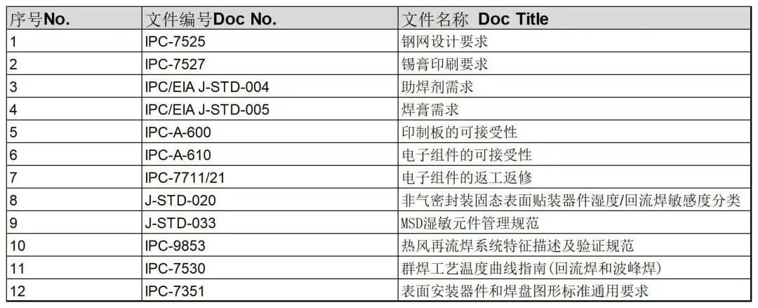
Cited Standards
|
|
Document No. |
Document Title |
|
1 |
IPC-7525 |
Stencil Design Guidelines |
|
2 |
IPC-7527 |
Solder Paste Printing Requirements |
|
3 |
IPC/EIA J-STD-004 |
Flux Requirements |
|
4 |
IPC/EIA J-STD-005 |
Solder Paste Requirements |
|
5 |
IPC-A-600 |
Acceptability of Printed Boards |
|
6 |
IPC-A-610 |
Acceptability of Electronic Components |
|
7 |
IPC-7711/21 |
Rework and Repair of Electronic Components |
|
8 |
J-STD-020 |
Moisture/Reflow Sensitivity Classification for Non-Hermetic Solid State Surface Mount Devices |
|
9 |
J-STD-033 |
MSD Moisture Sensitive Device Management Guidelines |
|
10 |
IPC-9853 |
Hot Air Reflow Soldering System Characteristics and Verification Guidelines |
|
11 |
IPC-7530 |
Guidelines for Temperature Profiles in Wave and Reflow Soldering |
|
12 |
IPC-7351 |
Generic Requirements for Surface Mount Device and Land Pattern Design |
-
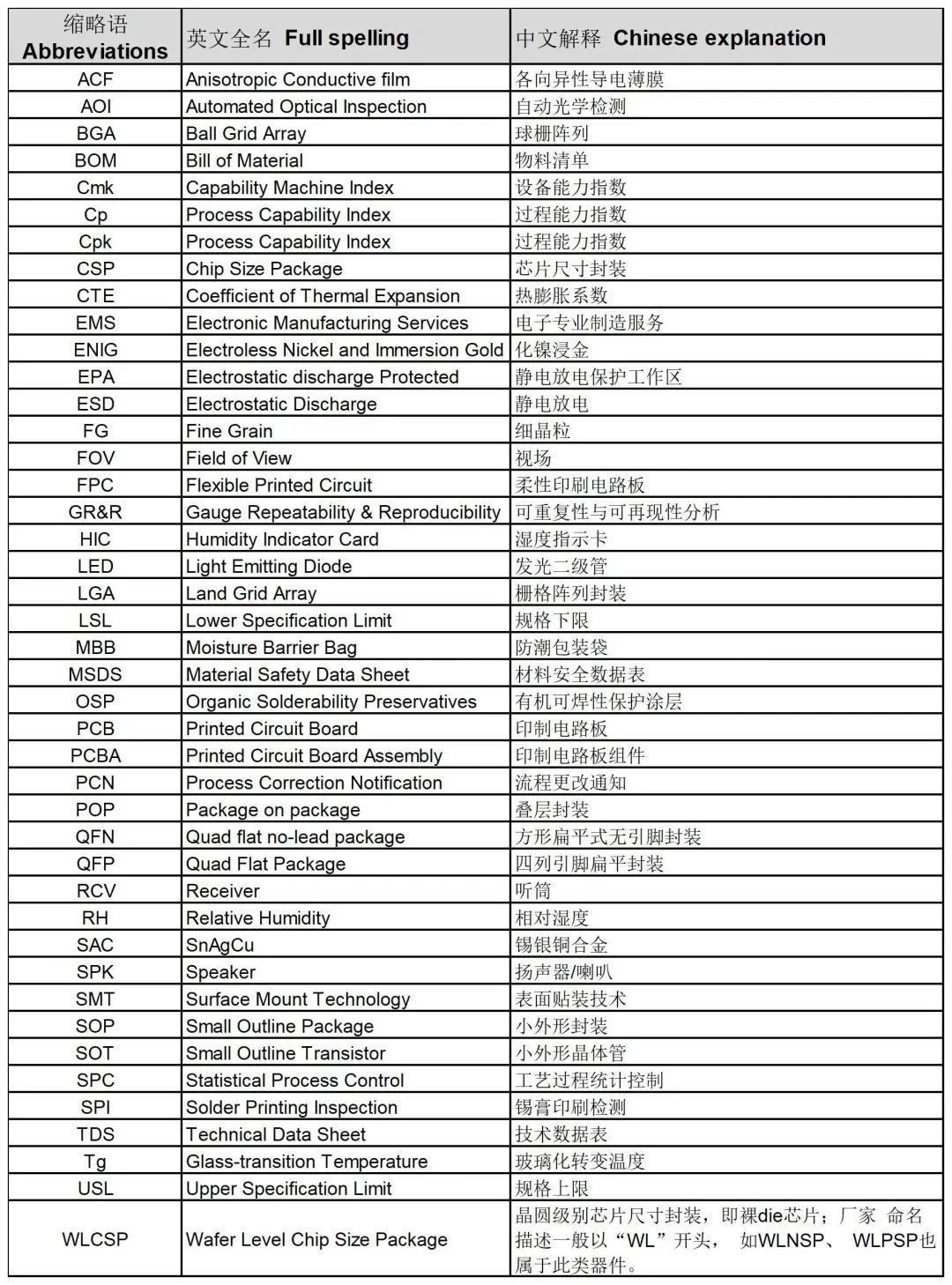
Terminology Abbreviations and Definitions
|
|
Full Spelling |
Chinese Explanation |
|
ACF |
Anisotropic Conductive Film |
各向异性导电薄膜 |
|
AOI |
Automated Optical Inspection |
自动光学检测 |
|
BGA |
Ball Grid Array |
球栅阵列 |
|
BOM |
Bill of Material |
物料清单 |
|
Cmk |
Capability Machine Index |
设备能力指数 |
|
Cp |
Process Capability Index |
过程能力指数 |
|
Cpk |
Process Capability Index |
过程能力指数 |
|
CSP |
Chip Size Package |
芯片尺寸封装 |
|
CTE |
Coefficient of Thermal Expansion |
热膨胀系数 |
|
EMS |
Electronic Manufacturing Services |
电子专业制造服务 |
|
ENIG |
Electroless Nickel and Immersion Gold |
化镍浸金 |
|
EPA |
Electrostatic Discharge Protected |
静电放电保护工作区 |
|
ESD |
Electrostatic Discharge |
静电放电 |
|
FG |
Fine Grain |
细晶粒 |
|
FOV |
Field of View |
视场 |
|
FPC |
Flexible Printed Circuit |
柔性印刷电路板 |
|
GR&R |
Gauge Repeatability & Reproducibility |
可重复性与可再现性分析 |
|
HIC |
Humidity Indicator Card |
湿度指示卡 |
|
LED |
Light Emitting Diode |
发光二级管 |
|
LGA |
Land Grid Array |
栅格阵列封装 |
|
LSL |
Lower Specification Limit |
规格下限 |
|
MBB |
Moisture Barrier Bag |
防潮包装袋 |
|
MSDS |
Material Safety Data Sheet |
材料安全数据表 |
|
OSP |
Organic Solderability Preservatives |
有机可焊性保护涂层 |
|
PCB |
Printed Circuit Board |
印制电路板 |
|
PCBA |
Printed Circuit Board Assembly |
印制电路板组件 |
|
PCN |
Process Correction Notification |
流程更改通知 |
|
POP |
Package on Package |
叠层封装 |
|
QFN |
Quad Flat No-Leads Package |
方形扁平式无引脚封装 |
|
QFP |
Quad Flat Package |
四列引脚扁平封装 |
|
RCV |
Receiver |
听筒 |
|
RH |
Relative Humidity |
相对湿度 |
|
SAC |
SnAgCu |
锡银铜合金 |
|
SPK |
Speaker |
扬声器/喇叭 |
|
SMT |
Surface Mount Technology |
表面贴装技术 |
|
SOP |
Small Outline Package |
小外形封装 |
|
SOT |
Small Outline Transistor |
小外形晶体管 |
|
SPC |
Statistical Process Control |
工艺过程统计控制 |
|
SPI |
Solder Printing Inspection |
锡膏印刷检测 |
|
TDS |
Technical Data Sheet |
技术数据表 |
|
Tg |
Glass-transition Temperature |
玻璃化转变温度 |
|
USL |
Upper Specification Limit |
规格上限 |
|
WLCSP |
Wafer Level Chip Size Package |
晶圆级别芯片尺寸封装,即裸die芯片;厂家命名描述一般以“WL”开头,如WLNSP、WLPSP也属于此类器件。 |
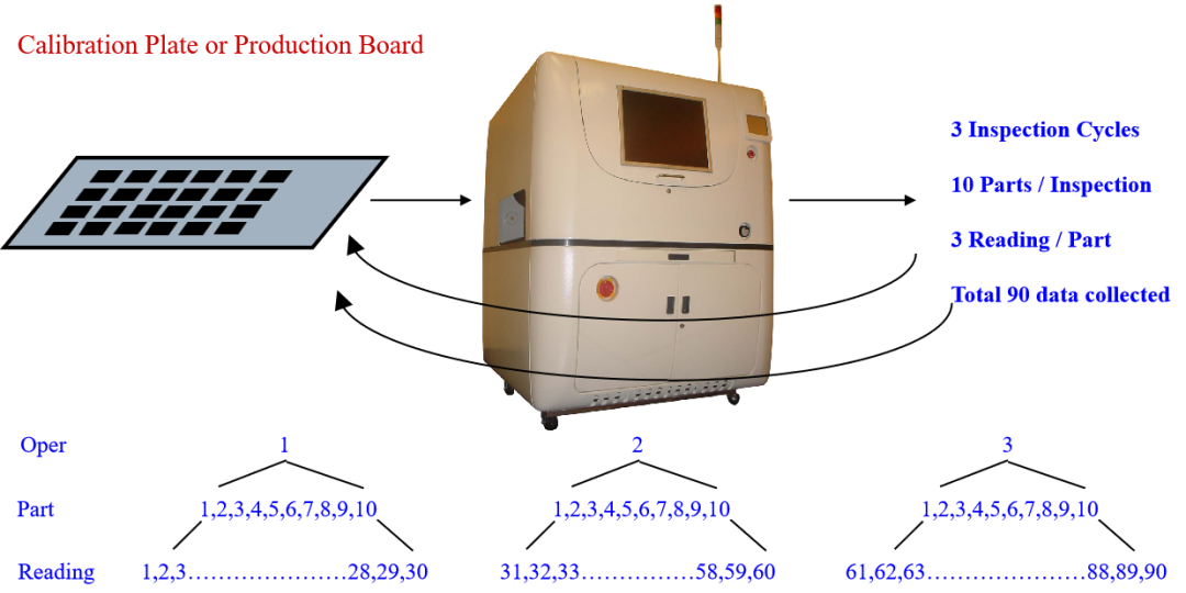
Reference ArticleLink: Work Instruction SOP丨SPI Printing Inspection Work SOP
Must configure online 3D SPI monitoring for solder paste printing quality.
Online SPI must have barcode scanning capability, SPI defect data must be saved for at least 3 months.
-
Before starting process optimization on the printer, the following requirements should be met:
-
Solder paste must meet J-STD-005 or equivalent requirements. -
The stencil should be in good condition and have the correct tension. -
The squeegee blade/printing head should be in good condition and correctly installed. -
During printing, there should be sufficient pin or fixture support for the PCB/FPC. -
Both sides of the stencil and the inside of the openings should be clean (checked with a microscope).
Online SPI equipment must meet the general requirements in the table below. Level II requirements apply to products containing devices with 0.4mm pitch/0201 and above, while Level I requirements apply to products containing devices with 0.3/0.35mm pitch/01005 and above.
Reference ArticleLink: PCBA Manufacturing Process Specification: SPI Demo (Benchmark Selection) Evaluation Report
|
No. |
Item |
TechnicalSpecifications |
Specification Requirements |
|
II Level Requirements |
I Level Requirements |
||
|
1 |
PCB Handling Capability |
PCB measurable range (length×width) |
50×50~450×535mm(single track) 50×50~450×250mm(double track) |
|
PCB Thickness |
0.4~4mm |
||
|
PCB Warpage Automatic Compensation Amount |
±5mm(the machine can automatically extend and retract) |
||
|
PCB Weight |
2.5KG |
||
|
Panel Independent Detection Function |
Can separately identify the mark points on the panel, preventing irregularities from causing mismeasurement |
||
|
2 |
Precision Requirements |
Barcode scanning (optional) |
The camera can identify one-/two-dimensional barcodes; if a barcode is not read, parameters can be set to decide whether to continue testing |
|
Camera |
Resolution25um |
Resolution20um |
|
|
Minimum Measurement Size |
Square: 200um Round: 250um |
Square: 150um Round: 200um |
|
|
Detection Capability |
0201 |
01005 |
|
|
ZAxis Resolution |
1pmbelow |
0.6umbelow |
|
|
HighPrecision |
2pm |
||
|
Volume Repeatability |
<3%@3σ |
||
|
Machine StabilityGR&R |
Solder Paste Thickness Measurement≤10% Solder Paste Area Measurement≤10% Solder Paste Volume Measurement≤10% |
||
|
3 |
Measurement Item Requirements |
Excess solder, insufficient solder, bridging, pulling tips, poor shape |
100% defect detection(according to testing principles) |
Requires editing test applications using GERBER files to generate test files and allows for offline programming; SPC software must be able to output solder paste thickness, volume, area, solder paste 3D graphics, solder paste 2D graphics, X/Y offset graphics, thickness distribution statistics overlay graphics, CPK distribution, single-point SPC graphics.
Every product produced online is inspected, and the solder paste quality CPK values are recorded every two hours.
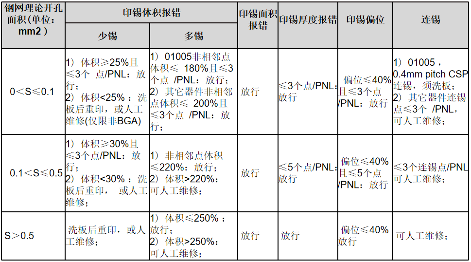
When conducting solder quality inspections, focus on detecting solder misalignment, solder paste volume, and solder paste area transfer rates according to the following requirements.
Reference ArticleLink:
PCBA Manufacturing Process Specification: FG Nano Printing Stencil Opening Area Ratio and Solder Paste Transfer Rate Relationship Study
The solder volume and area must refer to the specifications in the table below; if exceeded, the PCB must be cleaned and solder parameters adjusted. Solder quality requirement Cpk≥1.33; prioritize solder paste volume transfer rate data.
|
|
A Class |
B Class |
C Class |
D Class |
E Class |
|
|
0<S≤0.05 |
0.05<S≤ 0.1 |
0.1<S≤0.5 |
0.5<S≤1.5 |
S>1.5 |
||
|
Volume Specification Limits (%) |
LSL |
25% |
40% |
40% |
40% |
40% |
|
USL |
150% |
180% |
200% |
200% |
200% |
|
|
Area Specification Limits (%) |
LSL |
40% |
40% |
40% |
60% |
60% |
|
USL |
150% |
180% |
180% |
200% |
200% |
Reference ArticleLink: PCBA Manufacturing Process Specification: SMT Solder Paste Usage Algorithm and SPI Parameter Setting Standards (Algorithm Formula)
Solder Thickness Warning Threshold Requirements Table
|
|
|
|
|
|
|
|
|
|
|
|
|
|
|
|
|
|
|
|
|
|
|
|
|
|
|
|
|
|
|
|
|
|
|
|
|
|
|
|
|
|
|
|
|
|
|
|
|
|
|
|
5.1 GRR refers to the repeatability and reproducibility of measurements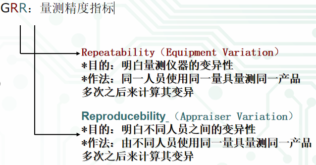
5.2 Common Measurement Control Chart Comparison
|
|
Name |
Advantages |
Disadvantages |
| X-R Chart |
Mean / Range Control Chart |
○ Easy to calculate ○ Can better estimate the process |
Process estimation is worse than X-s Chart |
|
X-R Chart |
Median / Range Control Chart |
○ Simple calculation | Process estimation is worse than X-R Chart |
|
X-s Chart |
Mean / Standard Deviation Control Chart |
○ Most accurate for estimating the process | Complicated calculation |
|
X-Rm Chart |
Individual Value/Moving Range Control Chart |
○ Simple calculation ○ Suitable for destructive, solvent density testing, or difficult measurements |
Small sample size, least able to estimate the process |
|
p Chart |
Defective Rate Control Chart |
○ Can be used with varying sample sizes ○ Can directly inspect defect rate trends |
Control limits calculation is complicated, and each point must be calculated. |
|
np Chart |
Defect Number Control Chart |
○ Used with constant sample sizes ○ Can directly inspect defect number trends |
If deliberately specified the same sample size, it may cause missed defects. |
|
u Chart |
Unit Defect Count Control Chart |
○ Can be used with varying sample sizes ○ Can directly inspect unit defect occurrence trends |
Control limits calculation is complicated, and each point must be calculated. |
|
c Chart |
Defect Count Control Chart |
○ Used with constant sample sizes ○ Can directly inspect defect occurrence trends |
If deliberately specified the same sample size, it may cause missed defects. |
5.3 Common SPC Control Techniques for SPI
-
Mean Control Chart (X Bar Chart).
-
Range Control Chart (R Chart)
-
Standard Deviation Control Chart (S Chart).
-
Process Capability Index, Cp
-
Process Precision, Ca (or K)
-
Process Comprehensive Capability Index, Cpk
5.4 Important Terminology Explanations
-
Upper/Lower Specification Limits (USL/LSL)
-
Upper/Lower Control Limits (UCL/LCL)
-
Standard Deviation (Sigma)
-
Process Capability Index-Cp
-
Process Precision-Ca
-
Process Comprehensive Capability Index-Cpk
Upper Specification Limit USL – The generated procedure is organized through the average values of various samples, according to statistical methods, to set the upper specification limit for shipment. (The same principle applies to the lower specification limit);
Upper Control Limit UCL – The generated procedure is based on sampling inspections of the product average values, plus the standard deviation of the distribution dispersion. SPI standard is 3 SIGMA;
Standard deviation is often used in probability statistics as a measure of statistical analysis (statistical dispersion);
In simple terms, standard deviation is a measurement concept of how much a set of values is dispersed from the average value. A larger standard deviation indicates that most values differ significantly from the average; a smaller standard deviation indicates that these values are closer to the average.
5.5 What is the best standard deviation
-
Besides quality, cost is also a key consideration for the survival of enterprises
Defect Rate PPM Calculation: The number of defects produced in every million inspected samples
| Sigma Level + – kσ | Cp Cpk | Yield % | Defect Rate ppm |
|
|
|
|
|
|
|
|
|
|
|
|
|
|
|
|
|
|
|
|
|
|
|
|
|
|
|
|
|
|
5.5 How to Determine Cpk Quality
-
The larger the Cpk value, the better the process capability
Grade Determination: Based on the size of the Cpk value, it can be divided into five levels
|
Level |
Cpk Value |
Handling Principles |
|
A+ |
1.67 ≦ Cpk |
No defects, consider reducing costs |
|
A |
1.33 ≦ Cpk ≦ 1.67 |
Maintain status quo |
|
B |
1 ≦ Cpk ≦ 1.33 |
Defects occur |
|
C |
0.67 ≦ Cpk ≦ 1 |
Immediate review and improvement |
| D | Cpk ≦ 0.67 | Take emergency measures, improve quality, and discuss specifications |

Advertising Space Recruitment:
Recruitment Phone:150 9990 5300
Recruitment WeChat: SMTDFM

Spread knowledge, empower intelligent manufacturing;
If helpful, it is an honor!
END
▼Click the card below to discover more wonderful articles
You“Looking”吗