Skip to content
The reliability testing and failure analysis of PCB / PCBA proceed hand in hand; when design pressures reach their limits, thorough inspection and analysis are needed to determine their failure modes. Some of these tests and potential failure causes are handled by manufacturers, as they may arise during the bare board manufacturing process, while other potential issues of PCBA should be addressed by the design team during prototyping and design validation. High-reliability designs, such as those in avionics and defense, may require extensive environmental testing and certification to ensure they function in the expected environments.
To start discussing this topic, it is important to understand the qualification aspects that will govern your bare board design and PCBA. We will explore various aspects of PCB/PCBA reliability, as well as some standard failure analysis techniques used to identify potential design change requirements.
Overview of PCB Reliability Testing Standards
Reliability testing broadly involves exposing a PCB or finished PCBA to extreme environmental conditions (thermal, corrosive, humidity, etc.) and then performing performance tests to ensure the device can withstand these conditions. In the field of reliability testing, there are many potential sources of stress on PCBs and finished PCBAs:
-
Mechanical loads (static load, vibration, and shock testing under MIL-STD/IPC/SAE standards)
-
Thermal or climatic loads (thermal flux under IPC-TM-650 2.6.7 and MIL-STD-202G, extreme temperatures, thermal shock; thermal cycling under MIL-STD-883 Method 1011, IPC-9701A [6], and JEDEC JESD22-A106)
-
Electrical loads (high power, derating verification, EMC, all in compliance with IPC/IEC/SAE standards) and UL compliance
-
Chemical loads (corrosion or other chemical exposures to match deployment environments)
-
Exposure to ionizing radiation (calculated as total ionizing dose (TID))
-
Contact with dust, particulates, and liquids
-
Accelerated aging tests for electronic components (HALT, HASS, HATS, etc.)
What Does Reliability Testing Involve?
PCB reliability assessment requires a set of tests for each of the areas mentioned above. Manufacturers will perform basic manufacturing board tests on your laminate, and they should be able to demonstrate that the bare board meets the requirements specified in your PCB manufacturing specifications. For PCBA, testing and reliability can be broader. Your manufacturer/assembler will perform their own series of tests and inspections to verify compliance with IPC product categories and basic IPC standards on the bare board, but more specialized tests (environmental or chemical testing) are typically run by the design team or contract testing companies to validate reliability in design.
Any guidelines for testing in these areas will involve a series of articles, so I will not delve deeply into all aspects of reliability testing and validation. Standard documents provided by IPC, MIL-STD, SAE, NASA/DO, and other organizations offer guidance in this field, as well as specific procedures for conducting these tests. IPC-TM-650 contains standardized testing methods for PCBs, but the other documents mentioned may exceed the requirements of IPC-TM-650 for specific products and industries.
PCB Failure Analysis
Determining the limits of PCB reliability involves identifying failures and how they occur in the device. Once a circuit board fails, an investigation is needed, and failures may occur gradually due to cumulative damage (such as fatigue), irregular (random or intermittent), or suddenly (due to shock). In investigating failure modes, the application of the aforementioned tests involves applying cumulative stress to the PCBA until failure occurs (thermal, mechanical, and environmental), and then inspecting the board to locate and examine specific failures.
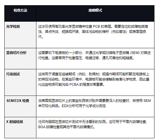
The table below matches standard PCB failure modes with inspection and failure analysis methods used in PCBs.
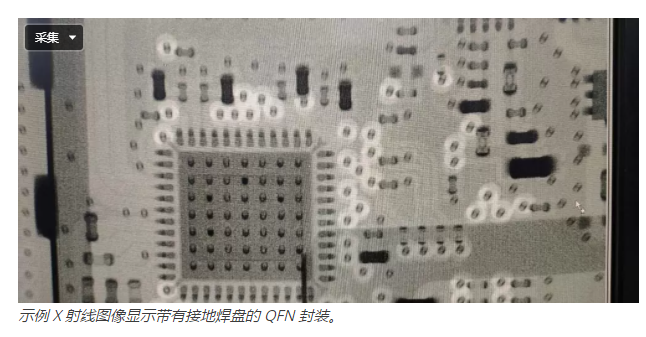
Identifying defects in these areas requires some skill. Some are obvious, such as extreme corrosion due to exposure to moisture, while others can only be seen by trained eyes. For example, identifying failures from X-ray images is not always clear due to the contrast and resolution of recorded images.
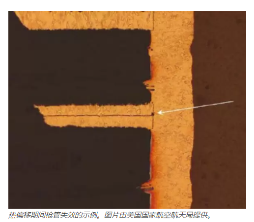
Similar conductive anodic filament failures can be easily detected due to high voltage or extended operation during the tube operation process, whether from a microscopic sample or from SEM images. With the right imaging techniques, both are clearly visible. For example, the image below shows a fracture clearly visible in a microscopic slice, which could lead to intermittent failures.
Once defects or failures are identified, steps should be taken to prevent the issues from occurring during operation or modify the design to make it more resilient to such problems. This must be handled on a case-by-case basis, depending on the type of defect and the mechanism leading to failure.
Final Thoughts
The key takeaway here is that no PCBA is invulnerable; any design may ultimately be subjected to stress until catastrophic failure occurs. If the stresses applied are so extreme that they are unlikely to be encountered during operation when deployed in the product’s intended environment, then you can consider your design successful from a reliability perspective. When testing reliability and investigating failures, it is necessary to consider the failure modes your device is most likely to encounter during operation and address these issues first.
Original text from: https://resources.altium.com/p/overview-pcbpcba-reliability-and-failure-analysis
Author: Zachariah Peterson
Note: This article is reproduced by 【射频学堂】, all original articles belong to the original author, sharing is intended for learning purposes. If there are any objections, please contact 【射频学堂】 to delete or modify. We wish you learn a lot and gain more in 【射频学堂】!
Group recruitment/reposting/cooperation/submission/promotion,
Contact RF Carpenter (WeChat ID: RF_Centered)
【RF Material Download】【RF Basics Essential】【Must-Read Articles
【射频学堂】 has started classes!
Scan the QR code to join the 【射频学堂】 knowledge community and receive RF knowledge anywhere, anytime!