As a hardware engineer, have you ever encountered these issues:
The circuit board shows no response after power is applied, like a “brick”.
The program occasionally starts, but sometimes hangs.
Peripheral initialization is abnormal, yet the code logic is correct.
These issues stem from startup process anomalies 80% of the time! Let’s learn about the STM32 startup mechanism and provide a hardware troubleshooting manual.
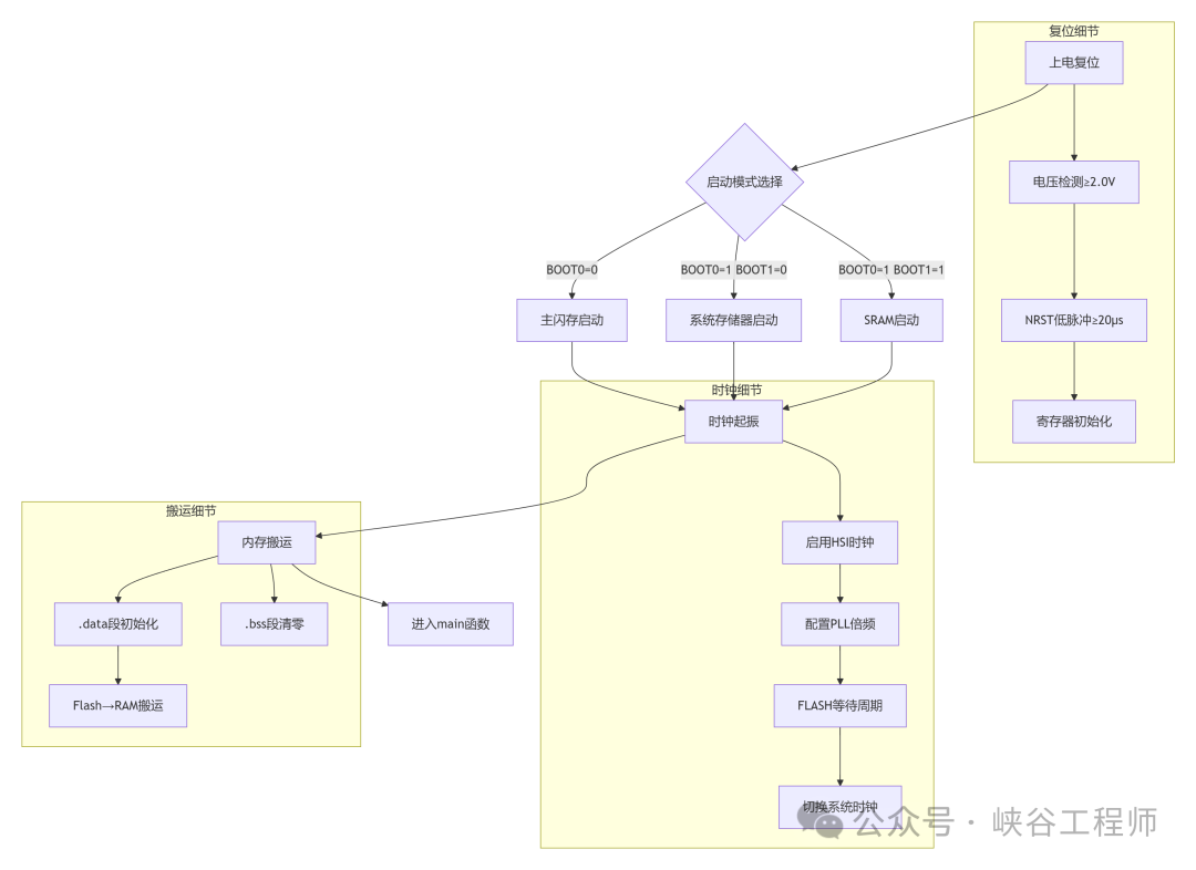 1. Power-On Reset
When power is applied, the reset circuit activates the NRST pin to pull low, and the internal voltage regulator starts to provide stable voltage for the core and memory. The clock tree initializes the HSI 8MHz internal clock to provide the reference first.
Internal reset process:
-
The power monitor (PVD) checks if the voltage reaches the 2.0V threshold.
-
The reset generator activates the internal 15kΩ pull-down resistor.
-
The reset signal maintains a low pulse for at least 20μs.
-
All registers (except the backup domain) are restored to their initial values.
A 10K pull-up resistor on the NRST pin must be connected to a 100nF capacitor externally; otherwise, ESD may cause an unexpected reset.
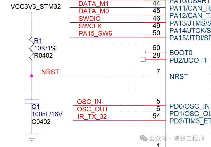
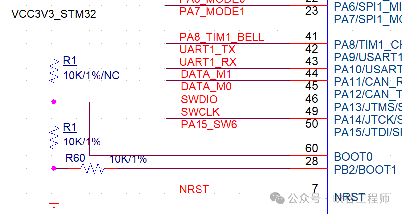
2. Boot Mode Selection
After the reset is released, the combination of the BOOT pins designed in the microcontroller hardware circuit will serve as a guide for code execution. The startup mode is determined by the level combination of the BOOT pins. The table below illustrates this:
| BOOT1 | BOOT0 | Startup Source | Typical Application |
| X | 0 | Main Flash | Normal program execution |
| 0 | 1 | System Memory | USB/IAP download |
| 1 | 1 | Built-in SRAM | Debugging/RAM testing |
In hardware design, BOOT1 is connected to a pull-up and a pull-down 10K resistor, while BOOT2 is fixed with a 10K resistor to GND.
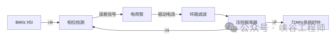
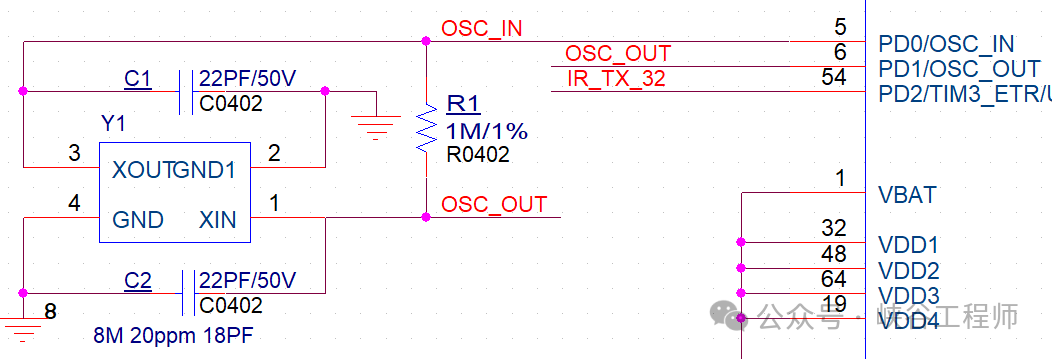
3. Clock Oscillation
The clock is the heart of the STM32, and the clock oscillation process determines whether the system can start normally. Over 40% of startup failures are related to the clock system.
Three-Level Clock Startup Process
| Stage | Clock Source | Key Actions | Typical Duration |
| Reset Initial Stage | HSI (Internal RC) | Basic operation of the core | 1-5μs |
| Clock Configuration | HSE (External Crystal) | Oscillator startup/stabilization | 1-15ms |
| System Operation | PLL (Phase-Locked Loop) | Frequency multiplication output system clock | 50-200μs |
Clock oscillation process:
-
After reset, the default state is that HSI is automatically enabled.
-
The external crystal oscillation process.
-
PLL configuration and switching.
Load capacitance calculation: C_load = (C1*C2)/(C1+C2) + C_stray
Recommended values for 16MHz crystal: C1=C2=22pF (need to be measured and adjusted)
PCB layout taboos:
-
Keep at least 5mm away from the power module.
-
Ground handling of clock signals.
-
Avoid right-angle traces.
Mastering the clock oscillation process is key to solving STM32 startup issues. Follow the method: check power → measure crystal → verify configuration → check status flags. This method can resolve 90% of clock-related failures.
4. Memory Management
When the clock system is ready, the core begins executing the relocation code in the startup file. Memory relocation refers to the process of copying initialized data from Flash to RAM (.data section) and zeroing the uninitialized data section (.bss). This process is completed by the assembly code in the startup file (startup_stm32xxxx.s), but it is supported by the precise storage architecture of the STM32.
Key Points of Bus Timing
| Parameter | Standard Value | Consequences of Hardware Exceeding Limits |
| Address Setup Time | 2.1ns | Data misalignment |
| Write Data Hold Time | 1.8ns | SRAM write failure |
| Bus Turnaround Cycle | 1.5ns | Bus conflict causing reset |
5. Startup Issue Troubleshooting Manual
Startup Anomaly Troubleshooting Guide
| Failure Phenomenon | Primary Checkpoint | Key Tools | Judgment Criteria |
| Completely unresponsive | NRST pin level | Oscilloscope + Multimeter | Voltage after release > 0.3×VDD |
| Repeated resets | Power ripple | Oscilloscope (AC coupling) | Vpp < 50mV @ 10MHz bandwidth |
| Random startup failures | Crystal oscillation amplitude | Oscilloscope ×10 probe | 0.3-0.8Vpp |
| Stuck in the initial startup phase | BOOT pin logic | Logic analyzer | Mode selection consistent with design |
| Memory access errors | VDDA/VREF+ voltage | High-precision multimeter | > 2.0V @ 3.3V system |
Hardware Design Testing Guidelines
| Check Item | Standard Requirements | Improvement Measures |
| Reset Circuit RC Parameters | R=10kΩ±5%, C=100nF±10% | |
| BOOT Pin Pull-Up Resistor | 4.7kΩ~10kΩ | |
| Crystal Load Capacitance Matching | Measured frequency deviation < 100ppm | Adjust C1/C2 ratio |
| Total Capacitance of VDD Decoupling Capacitors | ≥20μF | Add ceramic capacitors |
| Power Ripple (Vpp) | ≤50mV | Add π-type filter |
| NRST Wiring Length | ≤5cm | Adjust layout |