New Regulations Released, Industry Shocked
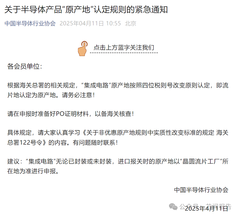
On April 11, 2025, the China Semiconductor Industry Association issued an urgent notice regarding the “Origin Determination Rules for Semiconductor Products,” which has sent ripples through the semiconductor industry. This notice has garnered significant attention because it clarifies the critical issue of determining the origin of integrated circuits, stipulating that the determination will be based on the wafer fabrication location. This rule may seem simple, but it has far-reaching implications across various levels, including international trade and corporate operations, closely tied to the interests of many companies in the industry, and sets the tone for a series of subsequent industry actions.
Rule Explanation: Why Wafer Fabrication Location
Four-Digit Tariff Code Change Principle
In international trade rules, the origin determination of “integrated circuits” follows the four-digit tariff code change principle. Simply put, it examines whether there is a change in the four-digit tariff item in the processing of goods. Wafer fabrication, as a key process in chip production, typically leads to changes in the tariff code from the manufacturing process of silicon wafers to wafers with specific circuit functions. For example, a standard silicon wafer originally corresponds to a primary raw material category, but after undergoing complex wafer fabrication processes, its tariff code changes to a category related to integrated circuits, reflecting a substantial change. Therefore, the wafer fabrication location becomes the core basis for origin determination. This determination method is based on the importance of the wafer fabrication process in altering the essential attributes of the product, with rigorous logic and legal basis, allowing for accurate definition of product origin and value-added stages in customs supervision and international trade statistics.
Customs Declaration Requirements
Regardless of whether the chips are packaged, customs declarations for imports must be based on the wafer fabrication location, which is a strict requirement. During declaration, companies must prepare PO (Purchase Order) documentation, which serves as proof of the production order. This documentation clearly displays the source order information for chip production, allowing customs to trace the chip production process and verify the accuracy of the wafer fabrication location declaration. For instance, if a company imports a batch of packaged chips, the customs declaration must be filled out based on the wafer fabrication location information, along with the PO documentation. If the wafer fabrication location is in Country A, and the declaration is filled out incorrectly or valid PO documentation cannot be provided, it may lead to customs clearance issues, resulting in goods being held up, fines, and impacting the efficiency and cost of the company’s supply chain.
Policy Background: An Inevitable Move in the Global Situation
Since 2025, the global semiconductor supply chain has been undergoing profound adjustments, as if stirred by an invisible hand. Countries like the United States have frequently taken action in the semiconductor field, imposing tariffs on imported semiconductor products in an attempt to gain dominance in this global semiconductor industry competition. In this context, origin determination is no longer a simple internal industry rule issue but has become a key factor affecting corporate tax burdens and industrial layout.
The U.S. tariff increases have put many semiconductor companies in a position of significantly increased costs. If the origin determination rules are ambiguous, companies may face high tariffs when importing, leading to decreased price competitiveness in the market and compressed profit margins. For example, a Chinese company importing wafers from Country A and packaging them in Country B may find that due to previously unclear origin determination rules, the U.S. could classify them as originating from a high-tariff region when imposing tariffs, forcing the company to bear high tariff costs, disrupting previously planned market strategies and profit expectations. As China is a major consumer market and manufacturing base for semiconductors, with a massive scale of semiconductor imports and exports each year, clarifying the wafer fabrication location as the origin rule acts like a “reassurance pill” for companies, helping them to reasonably plan their capacity layout. Companies can use this rule to comprehensively consider factors such as production costs, technological levels, and tariff policies in different regions, choosing the most advantageous wafer fabrication location to reduce tariff compliance risks and ensure stable operations in international trade.
Industry Impact: Opportunities and Challenges Coexist
Adjustment of Corporate Supply Chain Management
Under the new regulations, corporate supply chain management faces comprehensive adjustments. In the past, some companies did not pay enough attention to supply chain traceability management, leading to vague records in the wafer fabrication process when collaborating on integrated circuit production across multiple regions. Now, strengthening supply chain traceability management has become an urgent task. Companies need to establish detailed records of the wafer fabrication process, clearly indicating the location of wafer manufacturing plants, akin to affixing precise “identity labels” to every link in the supply chain, ensuring that declaration information aligns with actual production processes. For example, a chip company involved in production across multiple countries, which previously had scattered and unsystematic records for each link, has established an information management system after the new regulations were implemented, where information from raw material procurement, wafer fabrication processes to packaging and testing is recorded in real-time and accurately located, ensuring that wafer fabrication location information can be quickly and accurately provided during customs declaration.
At the same time, compliance in preparing declaration materials is also crucial. Preparing PO documentation, contracts for the wafer fabrication process, and production records in advance can effectively avoid delays in customs clearance due to incomplete materials. For instance, Company A, prior to the release of the new regulations, faced delays in customs clearance due to insufficient preparation of materials, having lacked the wafer fabrication process contract, resulting in goods being held at customs for a week, incurring additional storage costs and affecting downstream customer order deliveries. After the new regulations were released, Company A learned from this experience and established a declaration materials management team, starting to organize and prepare various declaration documents six months in advance, significantly improving customs clearance efficiency. Additionally, continuously monitoring policy dynamics is also a necessary course for companies. Organizing relevant personnel to study the “General Administration of Customs Order No. 122” and keeping abreast of the latest policy changes ensures that declaration work remains compliant, allowing for steady progress in the complex international trade environment.
Optimization of Industrial Layout
The wafer fabrication location becoming the core basis for origin determination has had a profound impact on the layout of the chip industry. It has prompted tighter integration across various links in the chip industry chain, driving overall optimization of the industrial layout. In the past, some companies may have primarily considered single factors, such as cost or technology, when choosing a wafer fabrication location. However, after the release of the new regulations, companies need to comprehensively consider multiple factors, such as tariff policies in different regions, industrial support capabilities, and levels of technological innovation. This has led to greater synergy among upstream and downstream companies in the chip industry chain when selecting locations, forming an industrial agglomeration effect.
For example, a region that originally had a relatively complete chip design industrial base but a relatively weak wafer fabrication process has increased support for the wafer fabrication industry after the new regulations were released, attracting several well-known wafer fabrication companies to settle there. These wafer fabrication companies closely collaborate with local design firms, achieving efficient integration of design and manufacturing processes, shortening product development cycles and reducing costs. Simultaneously, surrounding supporting industries such as photoresists and masks have also followed suit, further improving the local chip industry chain. This optimization of industrial layout enhances overall industry efficiency and competitiveness, giving the entire industry a greater advantage in global competition.
Changes in Market Competition Landscape
The implementation of the new regulations is also quietly changing the market competition landscape. For companies adopting the “design domestically, wafer fabrication abroad” model, special attention must be paid to the compliance declaration of the wafer fabrication location to avoid cost increases due to origin determination disputes. Some companies that previously held advantages in the international market may face the risk of losing market share to competitors if they cannot adapt to the new regulations in a timely manner and adjust their competitive strategies.
Some companies may adjust their competitive strategies, placing greater emphasis on cost control and technological enhancement in the wafer fabrication process. By optimizing wafer fabrication processes and improving production efficiency, they can lower costs to enhance product price competitiveness in the international market. Some companies may also increase their investment in wafer fabrication technology research and development, improving wafer fabrication technology levels to produce higher-performance chips that meet high-end market demands, thereby standing out in market competition. This series of strategic adjustments by companies will lead to a redistribution of market share. Some companies that adapt to the new regulations and actively transform are likely to capture a larger share of the market; while those that respond slowly and cannot adapt to the new regulations, especially small and medium-sized enterprises, may face survival challenges. Small and medium-sized enterprises, due to relatively limited resources in terms of funding and technology, may find it more challenging to cope with the declaration requirements and supply chain adjustments brought about by the new regulations. If they cannot timely obtain support and guidance from industry associations, governments, and other relevant parties, they may be eliminated in this market transformation.
Expert Opinions: Seizing Opportunities, Facing Challenges
Industry analyst Li Ming stated in an interview: “This new regulation further clarifies the technical determination standards for the origin of integrated circuits, acting like a beacon in the fog for companies, providing detailed operational guidance to address international trade barriers.” He pointed out that in the past, companies often found themselves in a passive position when facing complex and changing international trade policies due to unclear origin determination standards. For instance, when encountering anti-dumping investigations or tariff adjustments, it was difficult for companies to effectively protect their rights without accurately defining the origin. Now, with the new regulations clarifying the wafer fabrication location as the core basis for origin determination, companies can plan their production processes and supply chain layouts in advance around this standard, gaining a proactive position in international trade disputes.
For companies adopting the “design domestically, wafer fabrication abroad” model, Li Ming particularly reminded: “These companies must pay close attention to the compliance declaration of the wafer fabrication location; a slight oversight could lead to significant cost increases due to origin determination disputes.” He cited a well-known chip design company that previously faced high tariffs due to unfamiliarity with the declaration process for overseas wafer fabrication locations, resulting in a costly error in origin declaration during customs clearance, leading to high tariff payments and fines, which not only caused financial losses but also affected the company’s reputation. Therefore, these companies must strengthen their understanding and learning of the new regulations and strictly adhere to the declaration requirements.
Wang Qiang, a relevant person in charge of the China Semiconductor Industry Association, revealed in an interview: “In the future, the association will continue to closely cooperate with the General Administration of Customs to promote the establishment of clearer and more comprehensive origin determination rules.” He stated that as the global semiconductor industry continues to develop, with new technologies and business models emerging, existing origin determination rules may have ambiguous areas in certain special circumstances. The association will conduct in-depth research on the actual situation of the industry, collect feedback from companies, and discuss with the General Administration of Customs and other relevant departments to further refine the rules. For example, regarding emerging heterogeneous integrated chips, how to accurately define their wafer fabrication location and origin may require the formulation of specific rules. This will provide clearer direction for industry development and help maintain supply chain stability in the global division of labor. Companies should seize this opportunity to actively communicate with customs and industry associations, stay informed about rule changes, and optimize their capacity configuration. By collaborating with all parties to jointly address the complex and changing international trade environment, the Chinese semiconductor industry can steadily advance in global competition.
Conclusion and Outlook
The origin determination rules for integrated circuits released by the China Semiconductor Industry Association provide clear guidance for the industry in the complex international trade environment. The principle of determining based on the wafer fabrication location has profound significance for both the standardization of corporate customs declaration processes and the optimization of industrial layout. Companies should actively adapt to this new regulation, viewing it as an opportunity to optimize their development. Strengthening supply chain traceability management, ensuring compliance and completeness of declaration materials, monitoring policy dynamics, and timely adjusting business strategies are essential. At the same time, companies should enhance communication with customs and industry associations to jointly refine rule details. It is believed that with the joint efforts of all parties, the Chinese semiconductor industry can steadily advance in global competition and shine even brighter on the international stage. What do you think will be the biggest impact of this rule change on which companies? Feel free to leave your comments and discuss in the comment section.
Reference Documents:
1. Regulations on the Origin of Imported and Exported Goods of the People’s Republic of China
http://www.customs.gov.cn//customs/302249/302266/302267/3989417/index.html
2. Provisions on the Substantial Change Standards in Non-Preferential Origin Rules
http://www.customs.gov.cn/customs/302249/zfxxgk/hggzk/4101410/index.html

end
More information to come, stay tuned