(This article is translated from Semiconductor Engineering)
As the complexity of chips continues to increase, chip manufacturers are shifting from single-chip designs to multi-chip components, requiring more iterations, and the increasing level of customization makes design and verification work more time-consuming. Consequently, the first silicon tape-out success rate is sharply declining.
Details from a new functional verification survey highlight that developing advanced chips that are both functional and reliable is becoming increasingly difficult. In many cases, these chips are larger than the photomask-sized SoCs and integrate multiple components and wiring schemes, which may reduce their stability. Therefore, they require more optimization and more iterations.
These chips integrate more logic circuits, some of which are developed on different process nodes. They have more SRAM and more interconnect lines, both of which are evolving at a pace inconsistent with that of logic circuits. Additionally, they require more software support; for large language models (LLMs) and other AI algorithms, the pace of software development is much faster than that of hardware. They also need complex thermal management technologies, new materials, highly engineered and customized packaging, and more precise workload-related models. Worse still, they require more verification than the schedule allows.
The combined impact of all these factors is confirmed in the latest data. Harry Foster, Chief Verification Scientist at Siemens EDA, stated: “The entire industry is at an all-time low in achieving first silicon tape-out success. Historically, the success rate has been around 30%. Two years ago, from 2023 to 2024, this rate dropped to 24%. Now it has fallen to 14%. This is one data point. Another data point is that historically, we found that about two-thirds of projects are delayed, and now the rate of project delays has risen to 75%.”
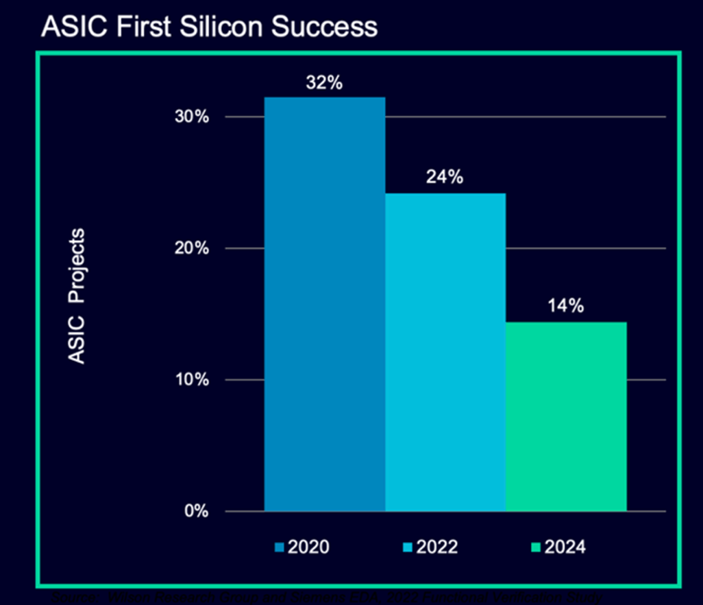
Figure 1: The number of designs that are functionally correct and manufacturable is declining.
(Image source: Siemens EDA/Wilson Research Group 2024 Functional Verification Study/DVCon)
In an increasingly complex and multi-layered design process, every step needs to improve production efficiency. Typically, this means hiring more engineers. Moreover, the extensive training required for engineers now far exceeds past requirements, making this impractical. This is why EDA vendors are so focused on integrating AI into their tools, essentially encoding relevant knowledge through reinforcement learning. However, this transition still takes time.
“Our approach has not worked,” Foster said. “We need to significantly improve production efficiency, but this is not a metric many people like to discuss because it is hard to measure. It is relatively easy to say, ‘this is 10% faster than that.’ Additionally, many companies lack the skills to manufacture very complex chips, or this is a new area for them. In the late 1990s, everyone was talking about the production efficiency gap. Now, this is the 2.0 version of the production efficiency gap. The issues now are different from 20 years ago, but there are also some common themes. We need to shift from isolated toolsets to more interconnected and integrated toolsets.”
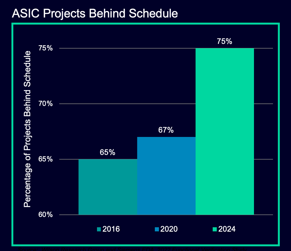
Figure 2: Increased complexity, coupled with the production efficiency gap, is slowing down chip manufacturing times.
(Image source: Siemens EDA/Wilson Research Group/DVCon)
However, the production efficiency issue cannot be entirely blamed on complexity. Even mainstream chip manufacturers are producing chips faster than in the past.
Matt Graham, Senior Group Director of Cadence Verification Software, stated, “Previously, we seemed to have some level of concern about first silicon success. But in the past year to year and a half, suddenly everyone is manufacturing more chips. Even companies that are not consumer market-focused, such as those making chips for testers, now have a demand for chip quantities that has quadrupled. They have gone from producing one chip every 18 months to now producing four to five chips a year. This is because everything has suddenly become more specialized.”
This situation often occurs during significant technological transitions, as processes, tools, and standards need to keep pace with the changes. “We often move from specialization to generalization and then back to specialization, and we seem to be in one of those cycles for specific applications,” Graham said. “This has led to everyone producing four to five times more chips, but no one has increased the corresponding workforce to handle the quadrupled number of tape-outs. If you are at the forefront of technology, with 3D-IC or chiplet-based designs, one wafer may need slight improvements.”
In cutting-edge technology areas, changes are profound and varied, sometimes differing by design, making it difficult to pinpoint the issues. Many of these designs are custom-tailored for large system vendors’ internal use, who are trying to push performance limits for specific applications or data types. In such cases, the cost of re-tape-out is part of the budgeting process, which also makes the relevant data somewhat ambiguous.
Frank Schirrmeister, Executive Director of Strategic Projects and System Solutions at Synopsys, stated, “For re-tape-out situations, logical functionality remains the most prominent issue. According to the Siemens EDA/Wilson Research Group survey, 70% of re-tape-outs are due to design errors caused by specification changes. This means someone misunderstood the specification requirements and sounded the alarm, leading to 50% of designs undergoing a second round of design. Some large chip manufacturers actually plan for up to four re-tape-outs. So ultimately, this is just a matter of complexity.”
This also creates significant potential opportunities for EDA companies, especially those that integrate some form of AI into their tools and design processes.
“In generative AI, you have a ‘co-pilot’ to assist and create,” said Sassine Ghazi, CEO of Synopsys, during a keynote at the Synopsys Users Conference. “With the ‘co-pilot’ technology we developed in collaboration with Microsoft, you have a workflow assistant, knowledge assistant, and debugging assistant. You can train a junior engineer and an expert engineer in a faster, more modern, and more efficient way to interact with our products. Then comes the creative part. We collaborate with customers early on, from RTL code generation, testbench generation to test assertions, where you can have a ‘co-pilot’ to help you create parts of RTL, testbench documentation, and test assertions.”
In some cases, production efficiency has been reduced from taking days in the past to just minutes now. But with the advent of intelligent agent-based AI, the biggest benefits are still to come, fundamentally raising the abstraction level of the entire design and verification process.
“As AI continues to evolve, workflows will change accordingly,” Ghazi said. “Our stakeholders often ask me when we will see AI bring changes to the EDA market. I believe that this will not happen unless workflows change. Only when you can do certain things in a fundamentally different way, delivering products faster, more effectively, and more efficiently, will you see change. Now, in the era of intelligent agent-based AI, agent engineers will collaborate with human engineers to tackle this complexity and change workflows.”
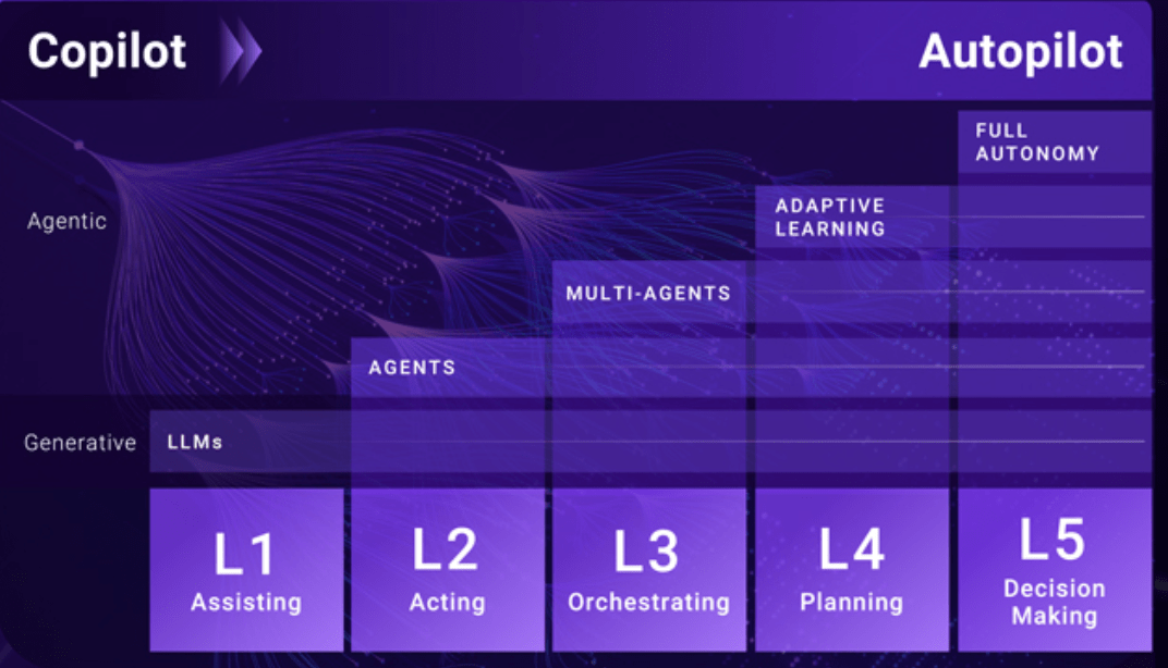
Figure 3: The evolution from generative AI to agent-based AI.
(Image source: Synopsys)
Abstract Issues
Some of the biggest challenges engineers face in advanced design are understanding the dependencies among hundreds or even thousands of different elements in the design. In the past, one key solution was to achieve tighter integration between hardware and software. Today’s co-design may involve dozens or even hundreds of small chips that need to work independently and sometimes collaboratively. To understand all possible interactions, multi-physics simulations are required, not just hardware-software co-design, and co-design now also includes various types of interconnects, packaging, photonics, and in some cases, larger-scale system architectures.
Moreover, all designs need to have design for testability (DFT), design for manufacturability (DFM), and sufficient yield (DFY), and there must be adequate internal controls to prevent overheating. If overheating occurs and aging is faster than expected, mechanisms for signal rerouting, primarily driven by software, need to be in place.
“In the verification domain, we see software increasingly becoming part of the complete solution,” Graham from Cadence said. “It’s not just ‘we want to make a chip.’ Today’s chips are application-specific. The end market and final application scenarios for the chips are clear. The software stack running on the chip is known, and there is also a clear understanding of the robots, cars, or other devices that will host the chip. We need to consider these factors from all angles, and we need to think about software verification, pre-manufacturing verification of the chip, and possibly even accelerate software work before putting it into a simulator or prototype platform.”
Initially, it is not always clear how much functionality should be attributed to software design and how much to hardware design. In complex designs, fine-tuning the balance between the two is a time-consuming process that easily leads to multiple redesigns.
“Software introduces a lot of functionalities and features,” said Ashish Darbari, CEO of Axiomise. “If the hardware team does not fully understand these functionalities, especially the verification team, then there will be a significant gap between what is tested and what is defined and planned. This is why many errors are missed. We do all these virtual prototyping and start software testing early to get thousands or tens of thousands of simulation vectors. But who will pay attention to the boundary conditions? In project after project, we find all these error cases in the first two to three weeks because the designers have run out of time.”
New Markets, Different Focuses
These issues extend far beyond functional verification and debugging, as functional verification and debugging have historically consumed the vast majority of chip development time and resources before manufacturing. The adoption of more complex chips in safety-critical applications such as automotive and military/aerospace presents entirely new requirements for design. In the past, these markets did not allow the use of advanced process chips because they were considered unreliable. However, with increasing competition from startups like BYD and NIO in China, as well as electric vehicle startups like Rivian and Lucid in the U.S., traditional automakers are racing to shift more functionality to software. This can only be achieved with more advanced chips and highly customized packaging, and as automakers move towards higher levels of automation, this will become increasingly necessary.
In these systems, safety is a mandatory requirement, but any system failure increases safety vulnerabilities. Therefore, chip designs need to consider more extreme conditions, from accelerated aging due to environmental heat in hot climates to real road conditions. While most of these scenarios can be tested through simulation, chips also need to undergo road testing. If certain issues cannot be adequately resolved through software, the chip needs to be redesigned.
“Functional verification will consume most of your time,” Darbari from Axiomise said. “But simple power optimization, such as introducing ‘don’t care’ (X) into the design, can easily make a module susceptible to Trojan attacks because these Xs now provide choices in the execution framework. So in the chip, an X is actually either 0 or 1. You cannot see the X, but from a simulation and behavioral perspective, these Xs now add comprehensive choices for the end user, allowing them to access design areas they should not. So on one hand, you need to perform functional verification. On the other hand, from a power consumption perspective, these X issues are introduced, leading to redundant areas. In terms of security, the larger the area on the chip, the higher the exposure risk.”
Integrating All Parts
Chips require additional chip area to accommodate more processing elements and more functionalities, or to house multiple small chips in certain types of advanced packaging. But this also makes achieving first silicon success more difficult.
“The accelerators you are dealing with have very complex workloads,” Foster from Siemens said. “This introduces a lot of non-determinism into the design, and we don’t even know how to semantically describe it, making verification very difficult. One of the challenges is that we have built many tool-centric processes without considering the feedback loops needed to optimize all these processes. In the future, we need more interconnected processes. This is how we can leverage AI. A clear example is when I am doing design for testability (DFT) and find, ‘Oops, I cannot meet the fault coverage requirements.’ So now I need to manually go back to the early stages of the tool process. All these loops need to be closed. But where do you find the people to do this?”
According to EDA companies and some leading foundries and OSATs, the answer lies in new tools, methodologies, possibly stricter design rules, and more limited packaging options. But it is still too early to judge how all this will ultimately develop. The pace of change is much faster than anyone predicted a few years ago, and the data is proof.
END