1. Surface Plating of Flexible Printed Circuit Boards (FPC)
(1) Pre-treatment for FPC Plating: The copper conductor surface exposed after the coating process of the flexible printed circuit board (FPC) may be contaminated with adhesives or inks, and may also have oxidation or discoloration caused by high-temperature processes. To achieve a tightly adhered plating layer, it is essential to remove the contaminants and oxidation layer from the conductor surface, ensuring it is clean.
However, some of these contaminants bond very firmly with the copper conductors, and weak cleaning agents may not completely remove them. Therefore, a combination of moderately strong alkaline abrasives and brushing is often used for treatment. Most adhesive coatings are epoxy resin-based, which have poor alkaline resistance, leading to a decrease in bonding strength. Although this may not be visibly apparent, during the FPC plating process, the plating solution may seep in from the edges of the coating layer, and in severe cases, this can cause the coating layer to delaminate. During final soldering, there may be instances where solder penetrates beneath the coating layer. It can be said that the pre-treatment cleaning process significantly impacts the fundamental characteristics of the flexible printed circuit board (FPC), and the treatment conditions must be given due attention.
(2) Thickness of FPC Plating: The deposition rate of the plated metal during electroplating is directly related to the electric field strength, which varies with the shape of the circuit pattern and the position of the electrodes. Generally, the narrower the wire width and the sharper the terminal points, the closer the distance to the electrode, resulting in a stronger electric field and a thicker plating layer in that area. In applications related to flexible printed circuit boards, there are often significant differences in wire widths within the same circuit, which can lead to uneven plating thickness. To prevent this, shunt cathode patterns can be added around the circuit to absorb the uneven current distribution on the plating pattern, maximizing uniformity in plating thickness across all areas.
Therefore, it is essential to focus on the structure of the electrodes. A compromise solution is proposed: for areas requiring high uniformity in plating thickness, strict standards should be applied, while standards for other areas can be relaxed. For example, the standards for lead-tin plating for soldering and gold plating for metal wire connections should be high, while the standards for lead-tin plating used for general corrosion protection can be more lenient.
(3) Stains and Dirt on FPC Plating: The state of the plating layer immediately after plating may appear normal, but soon after, some surfaces may show stains, dirt, or discoloration. This is particularly true if no abnormalities were detected during factory inspection, but issues arise during user acceptance checks. This is due to insufficient rinsing, leaving residual plating solution on the surface, which undergoes chemical reactions over time. Especially for flexible printed circuit boards, due to their softness and unevenness, various solutions can easily accumulate in the recesses, leading to reactions and discoloration in those areas. To prevent this, thorough rinsing and adequate drying treatment are necessary. High-temperature thermal aging tests can confirm whether rinsing was sufficient.
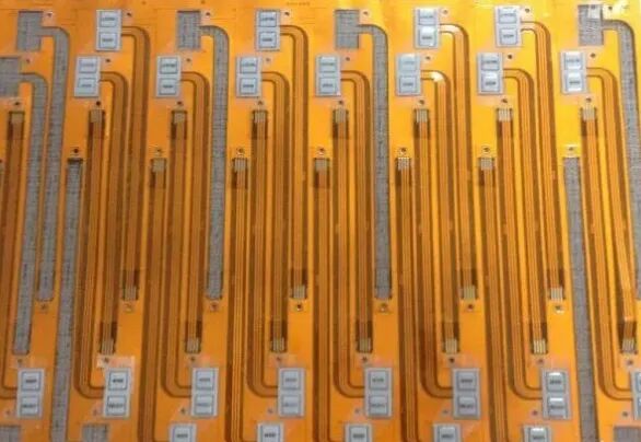
2. Chemical Plating of Flexible Printed Circuit Boards (FPC)
When the circuit conductors to be plated are isolated and cannot serve as electrodes, only chemical plating can be performed. Generally, the plating solutions used in chemical plating have strong chemical activity, with chemical gold plating being a typical example. The chemical gold plating solution is a highly alkaline aqueous solution with a very high pH value. When using this plating process, it is easy for the plating solution to seep beneath the coating layer, especially if the quality management of the coating lamination process is not strict, leading to low bonding strength and exacerbating this issue.
Due to the characteristics of the plating solution in displacement reaction chemical plating, it is more likely for the plating solution to penetrate beneath the coating layer, making it difficult to achieve ideal plating conditions with this process.
3. Hot Air Leveling for Flexible Printed Circuit Boards (FPC)
Hot air leveling was originally developed for coating lead-tin on rigid printed circuit boards (PCBs), but due to its simplicity, it has also been applied to flexible printed circuit boards (FPCs). Hot air leveling involves directly immersing the board vertically into a molten lead-tin bath, with excess solder blown away by hot air. This condition is very harsh for flexible printed circuit boards (FPCs); without any measures, they cannot be immersed in solder. The FPC must be clamped between a mesh made of titanium steel before being immersed in molten solder, and prior to this, the surface of the FPC must be cleaned and coated with flux.
Due to the harsh conditions of the hot air leveling process, it is also easy for solder to penetrate from the edges of the coating layer beneath the coating layer, especially when the bonding strength between the coating layer and copper foil is low, this phenomenon occurs more frequently. Since polyimide films are prone to moisture absorption, during the hot air leveling process, the absorbed moisture can rapidly evaporate due to the sudden heat, causing the coating layer to bubble or even delaminate. Therefore, prior to performing hot air leveling on FPCs, drying treatment and moisture control must be conducted.
This article is sourced from the internet, and the copyright belongs to the original author. If there is any infringement, please contact us for removal.
✦✧✦✧✦✧