WAGO project. The diagram on the left is the schematic & the one on the right is the physical image. They are consistent when viewed side by side.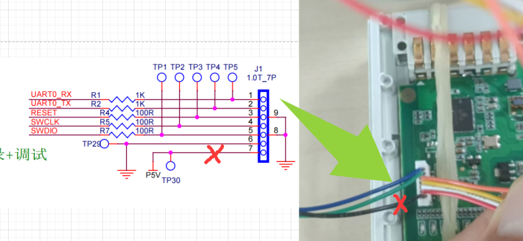 Please pay attention to the physical image on the right. I connected the 7PIN ribbon cable. The three wires on the left are for the serial port (ignore the 5V wire).The four wires on the right are for JLINK debugging. One GND is split to provide a GND for the left serial port analysis.The details are shown in the image below, which is the JLINK wiring.
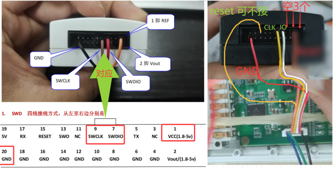 The source on the left is the J-LINK V11 documentation, which has excellent diagrams.The right side shows the physical wiring, mainly three wires. However, it does not have power supply capability; the MCU needs to be powered on to flash the bin.
 This wiring is actually quite troublesome. Just go to Lichuang and get an adapter board for free! It looks quite clear.https://oshwhub.com/ladeng/jlink-jie-kou-zhuan-jie-ban-zi-zhiOpen the webpage, place an order for zero yuan, and use yellow paint. Looking forward to the results.
 And it can test the built-in virtual serial port function of JLINK.The optimized wiring is shown below (when soldering, do not reverse the header pins).
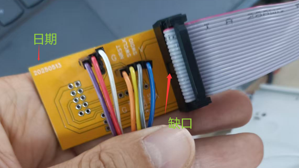 With this setup, a JLINK can simultaneously debug and view logs via UART!
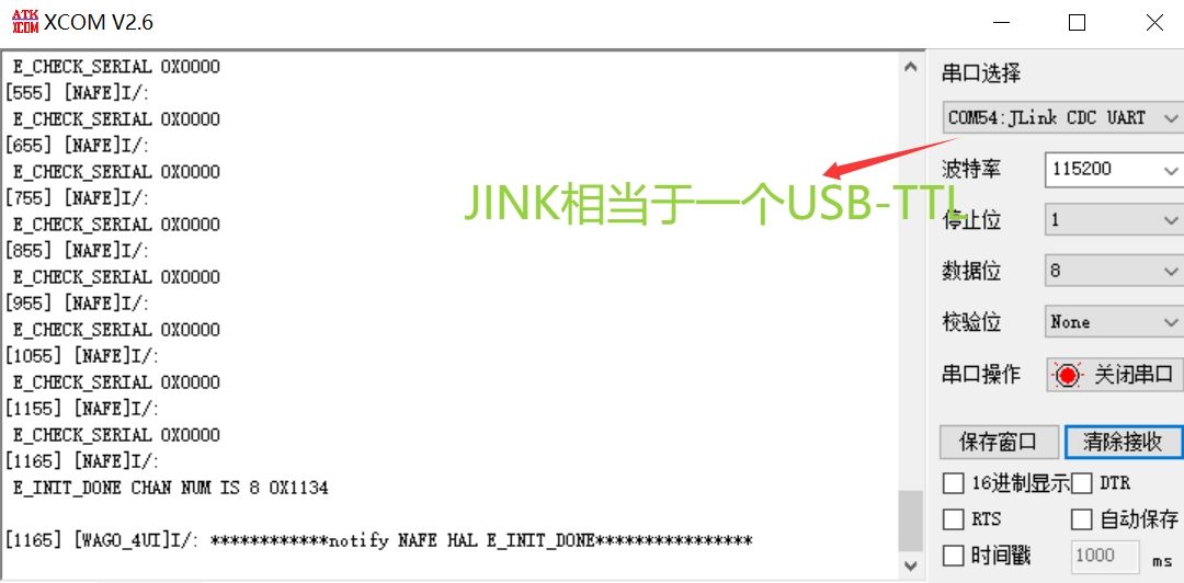