Microcontroller Introduction Tutorial 1: Basics of GPIO
1. Introduction
During the learning process, I increasingly feel the vastness and complexity of the knowledge system, which places high demands on memory and understanding. Each knowledge point is like a piece of a puzzle that requires our patience to assemble in order to construct a complete technical picture.
It is precisely because of this challenge that I have become more aware of the importance of systematic learning and timely summarization. Writing helps to organize my thoughts, deepening my understanding of knowledge and laying a solid foundation for future learning. This is my fundamental idea, currently in MD format (Typora).
1.1 Overview
As a student in electronic information (communication engineering), microcontroller technology is an important component of my studies. Writing this public account tutorial series is not only to document my learning journey and keep myself motivated, but also to consolidate the knowledge I have learned through writing, while improving my expression skills. If this process can also help friends who are exploring their learning paths, it would be even more meaningful, encouraging mutual supervision and progress!
Special Statement: The main reference is the STM32 introductory tutorial from Jiangsu University and the teachings of many technical experts on CSDN. The illustrations, schematics, and some technical explanations in this article may resemble those in these excellent tutorials, and I sincerely thank all the contributors who selflessly share knowledge!
The goal of this tutorial is to organize knowledge and record personal understanding during the learning process. Please feel free to point out any inaccuracies.
1.2 What is a Microcontroller?
A microcontroller (Microcontroller Unit, MCU) is a miniature computer system that integrates a CPU, memory, input/output interfaces, and other functions. It is widely used in embedded systems, such as smart home appliances, automotive electronics, industrial control, etc. In simple terms, it is a “small but complete” microcomputer.
1.3 Why Learn Microcontrollers?
•Pure Interest: When you see an LED blinking or a motor spinning, don’t you feel a sense of accomplishment? Haha!•Creating Fun Projects: Smart cars, pet robots, AI assistants, and all sorts of quirky gadgets… you can make whatever you think of!•The Joy of Hands-On Practice: No more just talking theory; you can see the actual effects of every line of code!•The Joy of Creation: You can realize various creative ideas with just a few bucks worth of chips!
Learning for the sake of interest makes the process more motivating and easier to persist!
1.4 Learning Path
This tutorial series will start from the basics of GPIO and gradually delve into advanced features such as timers, serial communication, and interrupts. It is recommended to learn in order, with each chapter containing theoretical explanations and practical projects.
About the Theoretical Part: I will try to use charts and diagrams to explain abstract concepts, allowing everyone to intuitively understand the working principles.
About Practical Projects: Each project will provide complete source code and detailed step-by-step instructions to ensure everyone can successfully replicate them.
2. Preparation
2.1 Hardware Preparation
STM32 Core Board: It must be the “Blue Pill” STM32F103C8T6 core board.
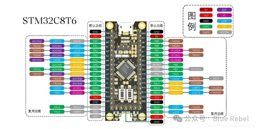
Figure 1: STM32F103C8T6 Core Board (Blue Pill)
USB to TTL Module: Used for program downloading and serial debugging.
ST-Link Debugger: Used for program downloading and online debugging.
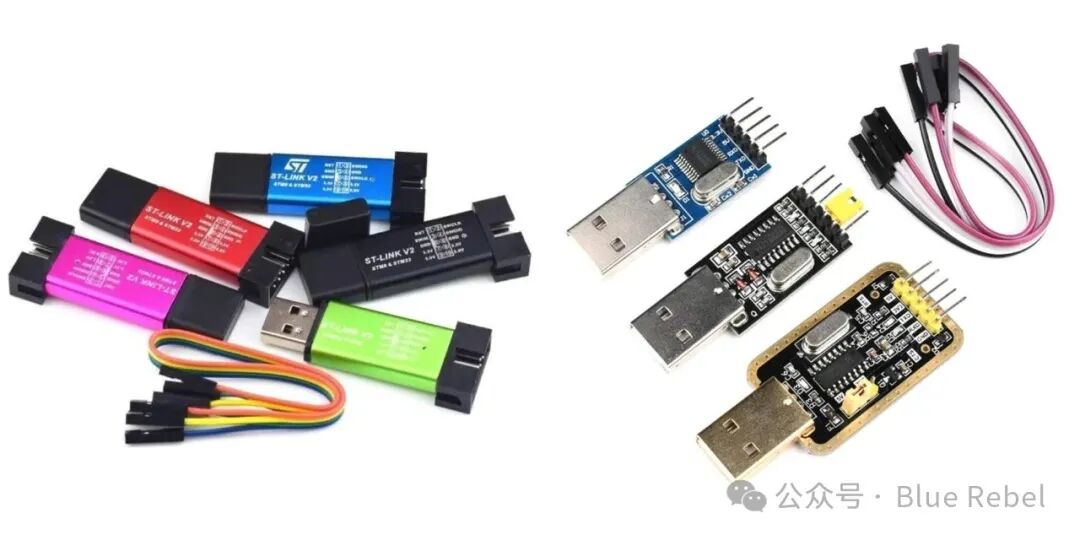
Figure 2: STLINK and CH340
Breadboard and Dupont Wires: Used for building experimental circuits.
Optional Expansion Modules: LED modules, button modules, buzzer modules, OLED displays, sensor modules, etc. You can choose according to your interests. Additionally, there are many STM32 beginner learning kits available online for around 80 yuan, which include commonly used modules and are sufficient for introductory learning.
2.2 Software Preparation
You need to download theKeil MDK5 development environment and relateddrivers. There are many online tutorials for software installation and environment setup, so I won’t repeat that here. This tutorial series mainly focuses onunderstanding principles and practical applications, and I recommend looking for other technical details on platforms like Bilibili, CSDN, and the official STM32 manuals—this is also a good opportunity to exercise your ability to gather information and solve problems!
3. Basics of GPIO
3.1 What is GPIO?
•GPIO (General Purpose Input Output) is a general-purpose input/output port•Can be configured in 8 different input/output modes•Pin levels: 0V~3.3V, some pins can tolerate 5V•In output mode, it can control the port to output high or low levels, used to drive LEDs, control buzzers, simulate communication protocol output timing, etc.•In input mode, it can read the high or low level or voltage of the port, used for reading button inputs, external module level signal inputs, ADC voltage collection, and receiving data from analog communication protocols, etc.
3.2 GPIO Port Organization Structure
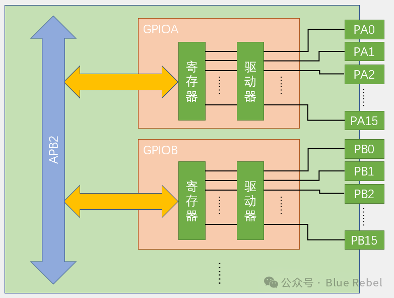
Figure 3: STM32 GPIO Port Organization Structure
3.2.1 Port Grouping Description
The GPIOs of STM32 are managed in groups by port:
GPIOA Port:
•Contains 16 pins from PA0 to PA15•Each pin has its own register and driver•Exchanges data with the CPU via the APB2 bus
GPIOB Port:
•Contains 16 pins from PB0 to PB15•Structure is identical to GPIOA•Also connected to the APB2 bus
Other Ports:
•Depending on the chip model, there may also be GPIOC, GPIOD, etc.•Each port is a 16-bit wide independent unit
3.2.2 Bus Connection Method
APB2 Bus:
•All GPIO ports are connected to the APB2 (Advanced Peripheral Bus 2)•APB2 is a high-speed peripheral bus suitable for GPIOs that require quick response•The CPU performs read and write operations on GPIO registers via the APB2 bus
Data Flow Direction:
•Output Direction: CPU → APB2 Bus → GPIO Register → Driver → Pin•Input Direction: Pin → Register → APB2 Bus → CPU
This grouping management method makes GPIO control more orderly, allowing each port to be configured and operated independently, enhancing the system’s flexibility and reliability.
3.3 Basic Structure of I/O Ports
Each GPIO has a circuit structure like this:
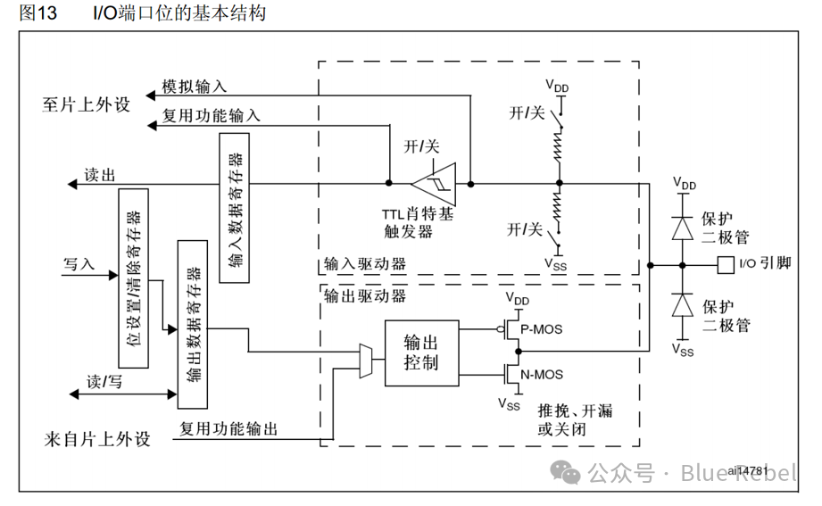
Figure 4: Basic Structure of I/O Ports
3.3.1 Circuit Composition Analysis
Protection Diodes: The diodes on both sides of the IO pin prevent excessive high or low voltage inputs from the outside. When the pin voltage exceeds VDD, the upper diode conducts; when the pin voltage is below VSS, the lower diode conducts, preventing abnormal voltages from damaging the chip. However, high-power devices should not be directly connected; isolation circuits are required.
P-MOS and N-MOS Transistors: The unit circuit composed of P-MOS and N-MOS transistors allows GPIO to have “push-pull output” and “open-drain output” modes. The two transistors work complementarily to achieve strong driving capability.
TTL Schmitt Trigger: After the signal passes through the trigger, the analog signal is converted into a digital signal of 0 and 1. When GPIO is used as an ADC input channel, the “analog input” function is used, and the signal does not pass through the trigger for conversion.
Important Note: In the GPIO table of the STM32 reference manual, pins marked “FT” are compatible with 3.3V and 5V; pins not marked “FT” are not compatible with 5V input.
4. GPIO Operating Modes of STM32
GPIO supports4 input modes and 4 output modes, and supports three maximum toggle speeds (2MHz, 10MHz, 50MHz).
Each I/O port can be programmed freely, but the I/O port registers must be accessed in 32-bit words.
4.1 List of 8 Operating Modes
| Mode Name | Nature | Features |
| Floating Input | Digital Input | Can read pin levels; if the pin is floating, the level is uncertain |
| Pull-Up Input | Digital Input | Can read pin levels; internally connected to a pull-up resistor, defaults to high level when floating |
| Pull-Down Input | Digital Input | Can read pin levels; internally connected to a pull-down resistor, defaults to low level when floating |
| Analog Input | Analog Input | GPIO is invalid; the pin is directly connected to the internal ADC |
| Open-Drain Output | Digital Output | Can output pin levels; high level is high impedance, low level connects to VSS |
| Push-Pull Output | Digital Output | Can output pin levels; high level connects to VDD, low level connects to VSS |
| Multiplexed Open-Drain Output | Digital Output | Controlled by on-chip peripherals; high level is high impedance, low level connects to VSS |
| Multiplexed Push-Pull Output | Digital Output | Controlled by on-chip peripherals; high level connects to VDD, low level connects to VSS |
4.2 Detailed Explanation of Input Modes
4.2.1 Floating Input Mode
In floating input mode, the level signal of the I/O port directly enters the input data register. The level state of the I/O is uncertain and is entirely determined by external input; if the pin is floating (no signal input), reading the level of that port is uncertain.
Characteristics: Neither pull-up nor pull-down resistors are connected, and the input signal is entirely determined by external factors.
4.2.2 Pull-Up Input Mode
In pull-up input mode, the level signal of the I/O port directly enters the input data register. When the I/O port is floating (no signal input), the input level can remain high.
Characteristics: The internal pull-up resistor is connected to high level, so pull-up input is commonly used to detect low levels.
4.2.3 Pull-Down Input Mode
In pull-down input mode, the level signal of the I/O port directly enters the input data register. When the I/O port is floating (no signal input), the input level can remain low.
Characteristics: The internal pull-down resistor is connected to low level, so pull-down input is commonly used to detect high levels.
4.2.4 Analog Input Mode
In analog input mode, the analog signal (voltage signal, not level signal) of the I/O port is directly input to on-chip peripheral modules, such as the ADC module.
4.3 Detailed Explanation of Output Modes
4.3.1 Open-Drain Output Mode
In open-drain output mode, the value is set/cleared through the bit setting register or output data register, passing through the N-MOS transistor, and finally outputting to the I/O port.
Working Principle:
•When the output is set tohigh level, the N-MOS transistor is in the off state, and the level of the I/O port is determined by external pull-up or pull-down.•When the output is set tolow level, the N-MOS transistor is in the on state, and the I/O port outputs a low level.
Characteristics: Can only output strong low levels; high levels must rely on external resistors to pull up. Suitable for current-type driving, with relatively strong current absorption capability (generally within 20mA).
4.3.2 Multiplexed Open-Drain Output Mode
Similar to open-drain output mode, except that the high and low levels output are not directly written to the output data register by the CPU, but are determined by the multiplexing function of on-chip peripheral modules.
4.3.3 Push-Pull Output Mode
In push-pull output mode, the value is set/cleared through the bit setting register or output data register, passing through both P-MOS and N-MOS transistors, and finally outputting to the I/O port.
Working Principle:
•When the output is set tohigh level, the P-MOS transistor is on, and the N-MOS transistor is off, outputting a high level at the I/O port.•When the output is set tolow level, the P-MOS transistor is off, and the N-MOS transistor is on, outputting a low level at the I/O port.
Characteristics: Can output strong high and low levels, connecting to digital devices. Not only does it have high and low levels, but during high levels, there will be strong current flowing through, which can drive some components.
4.3.4 Multiplexed Push-Pull Output Mode
Similar to push-pull output mode, except that the high and low levels output are not directly written to the output data register by the CPU, but are determined by the multiplexing function of on-chip peripheral modules.
5. Differences Between Push-Pull Output and Open-Drain Output
5.1 Push-Pull Structure
Push-pull structure refers to two transistors or MOSFETs with the same parameters controlled by two complementary signals, where one is always on while the other is off. The high and low levels are determined by the output level.
In operation, the two symmetrical power switch transistors are only on one at a time, resulting in low conduction loss and high efficiency. The output can both sink current to the load and source current from the load.
5.2 Main Differences
•Open-Drain Output: Can only output strong low levels; high levels must rely on external resistors to pull up. Suitable for current-type driving, with relatively strong current absorption capability (generally within 20mA).•Push-Pull Output: Can output strong high and low levels, connecting to digital devices.
6. GPIO Mode Selection Guide
6.1 Common Modes and Application Scenarios
•Floating Input (IN_FLOATING): Floating input can be used for button recognition, RX1.•Pull-Up Input (IPU): IO with internal pull-up resistor input.•Pull-Down Input (IPD): IO with internal pull-down resistor input.•Analog Input (AIN): Used for ADC analog input or low-power mode to save energy.•Open-Drain Output (OUT_OD): IO outputs 0 to GND, IO outputs 1 is floating, requiring an external pull-up resistor. Can read IO input level changes to achieve bidirectional functionality.•Push-Pull Output (OUT_PP): IO outputs 0 to GND, IO outputs 1 to VCC, reading input values is unknown.•Multiplexed Push-Pull Output (AF_PP): On-chip peripheral functions (I2C SCL, SDA).•Multiplexed Open-Drain Output (AF_OD): On-chip peripheral functions (TX1, MOSI, MISO, SCK, SS).
6.2 Most Common Modes
Push-Pull Output and Pull-Up Input are the two most commonly used modes.
7. Project Example – Running LED
By controlling the sequential lighting of LEDs, we can verify the GPIO output function and achieve a cool running LED effect.
7.1 Hardware Connection
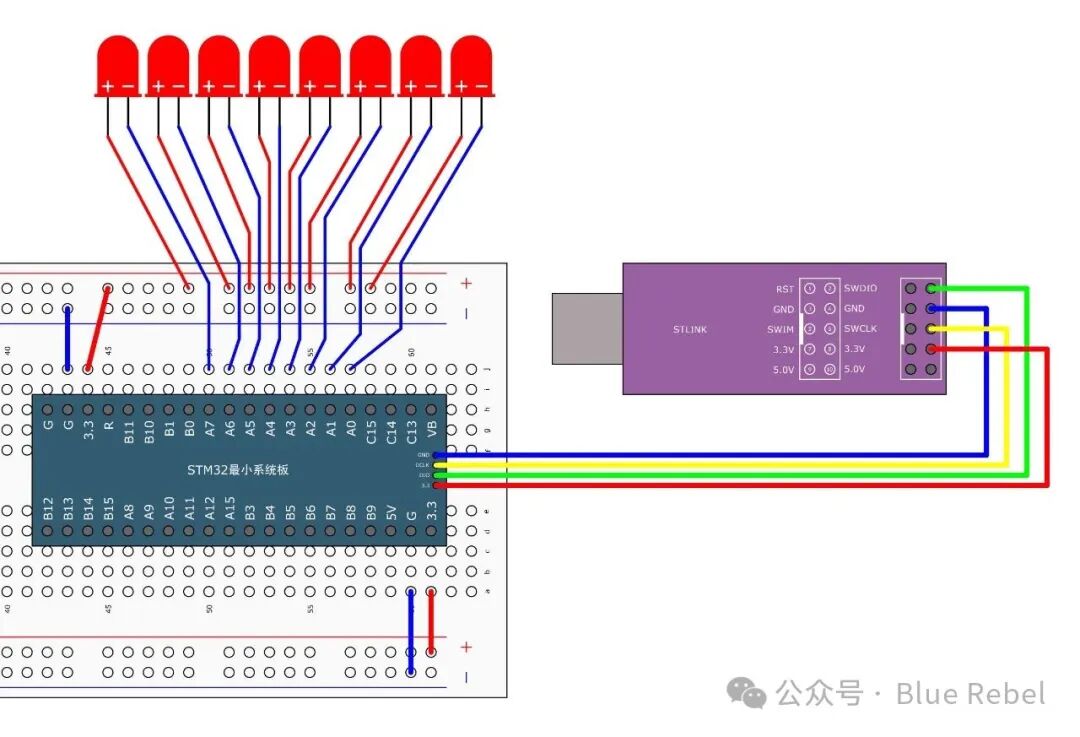
Figure 5: Hardware Connection Diagram for Running LED
7.2 Code Implementation
#include "stm32f10x.h"                  // Device header#include "Delay.h"
int main(void){    /*Enable clock*/    RCC_APB2PeriphClockCmd(RCC_APB2Periph_GPIOA, ENABLE);    //Enable clock for GPIOA                                                            //Clock must be enabled before using peripherals, otherwise operations on peripherals will be ineffective.
    /*GPIO Initialization*/    GPIO_InitTypeDef GPIO_InitStructure;                    //Define structure variable
    GPIO_InitStructure.GPIO_Mode = GPIO_Mode_Out_PP;        //GPIO mode, set to push-pull output mode    GPIO_InitStructure.GPIO_Pin = GPIO_Pin_All;                //GPIO pins, set to all pins    GPIO_InitStructure.GPIO_Speed = GPIO_Speed_50MHz;        //GPIO speed, set to 50MHz
    GPIO_Init(GPIOA, &GPIO_InitStructure);                    //Pass the assigned structure variable to GPIO_Init function                                                            //The function will automatically configure the corresponding registers based on the structure parameters                                                            //Initialize GPIOA
    /*Main loop, the code inside the loop will execute continuously*/    while (1)    {        /*Use GPIO_Write to set the high and low levels of all GPIOA pins, achieving the running LED effect*/        GPIO_Write(GPIOA, ~0x0001);    //0000 0000 0000 0001, PA0 pin is low, other pins are high, note that the data is bitwise negated        Delay_ms(50);                //Delay 50ms        GPIO_Write(GPIOA, ~0x0002);    //0000 0000 0000 0010, PA1 pin is low, other pins are high        Delay_ms(50);                //Delay 50ms        GPIO_Write(GPIOA, ~0x0004);    //0000 0000 0000 0100, PA2 pin is low, other pins are high        Delay_ms(50);                //Delay 50ms        GPIO_Write(GPIOA, ~0x0008);    //0000 0000 0000 1000, PA3 pin is low, other pins are high        Delay_ms(50);                //Delay 50ms        GPIO_Write(GPIOA, ~0x0010);    //0000 0000 0001 0000, PA4 pin is low, other pins are high        Delay_ms(50);                //Delay 50ms        GPIO_Write(GPIOA, ~0x0020);    //0000 0000 0010 0000, PA5 pin is low, other pins are high        Delay_ms(50);                //Delay 50ms        GPIO_Write(GPIOA, ~0x0040);    //0000 0000 0100 0000, PA6 pin is low, other pins are high        Delay_ms(50);                //Delay 50ms        GPIO_Write(GPIOA, ~0x0080);    //0000 0000 1000 0000, PA7 pin is low, other pins are high        Delay_ms(50);                //Delay 50ms    }}
This section on GPIO has been briefly introduced.
8. References
The writing process references the following excellent resources:
1.Jiangsu University STM32 Introduction Tutorial (my microcontroller white moonlight, very well explained!!)2.Quick Start with STM32 Development from Scratch (Step-by-Step Guide) – CSDN Blog[1]3.Detailed Explanation of STM32 GPIO – Blog Park[2]4.STM32F103x Data Sheet – Official Technical Document5.STM32 Chinese Reference Manual V10 – Detailed Register Descriptions
Writing Tool: This tutorial is written in Markdown format, completed using the Typora editor, and later converted for public account publication.
References
<span>[1]</span> CSDN Blog: https://blog.csdn.net/yychuyu/article/details/134380570<span>[2]</span> Blog Park: https://www.cnblogs.com/Sharemaker/p/17107060.html