Have you ever thought that the reason your thin and light smartphone can run smoothly and has long battery life might be due to a black technology called “SOI”? It acts like a magical “sandwich” for the core of the chip, fundamentally changing the underlying structure of the chip.
Today, let’s unveil the secrets of this “sandwich”!
1. Why create a “sandwich”?
In traditional chips, all transistors are directly placed on a pure silicon substrate. You can imagine it as all the “residents” crowded onto a large foundation, where circuits easily “visit” each other, causing interference that leads to high power consumption and slow speeds.
Especially in the 1980s, a more advanced SOS technology was prohibitively expensive and could not be used for civilian purposes. Thus, scientists had a brilliant idea: what if we placed an excellent “insulating floor” between the silicon substrate and the transistors?
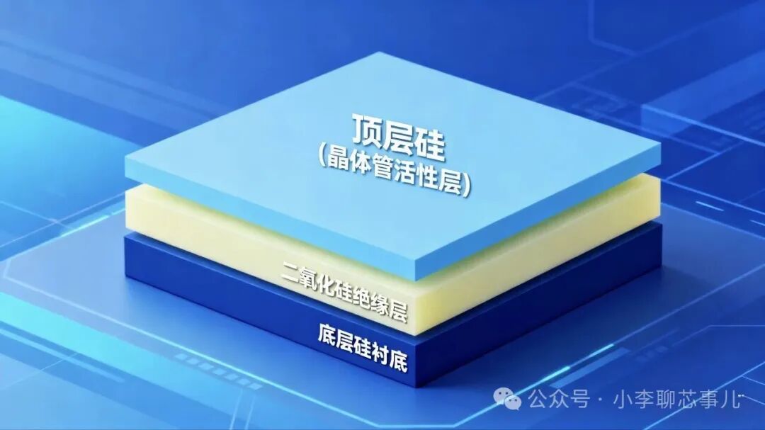
This is the origin of SOI technology! Its structure resembles a sandwich: top layer silicon (the active layer for making transistors) – silicon dioxide insulating layer – bottom layer silicon substrate. This “insulating floor” can effectively isolate interference, allowing chip performance to soar!
Core benefits: faster speeds, lower power consumption, and stronger radiation resistance, perfectly meeting the needs of high-end smartphones, aerospace, and other fields.
2. How is this “chip sandwich” manufactured?
The challenge arises: it is impossible to directly “grow” single crystal silicon on a smooth oxide layer. Three major technologies in the industry come into play, each showcasing its unique capabilities:
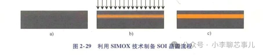
1. “Ion Implantation” Method (SIMOX) – Embedded Mastery
Method: Like using a high-energy “ion gun” to force a large number of oxygen ions into the silicon wafer, followed by high-temperature “annealing” to allow oxygen and silicon to react internally, forming a buried silicon dioxide insulating layer.
Advantages: Uniform insulating layer, controllable thickness.
Disadvantages: Similar to an internal injury treatment, it can damage the top layer of silicon, and the insulating layer cannot be made thick, resulting in high costs. It can be understood as an early-generation technology, good but expensive and limited.
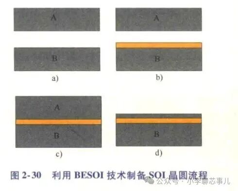
2. “Glue Bonding” Method (BESOI) – Physical Bonding Technique
Method: Prepare two wafers, one coated with an oxide layer as the “insulating sandwich” and the other as the “top layer bread”. Use a special “silicon fusion bonding” technology (similar to high-temperature strong glue) to tightly bond them, then grind the “top layer bread” to an extremely thin thickness.
Advantages: The quality of the top layer silicon is excellent, and the insulating layer is a high-quality thermal oxide film with a large adjustable thickness range.
Disadvantages: The grinding process is extremely wasteful of materials, high cost, and difficult to control thickness uniformity.
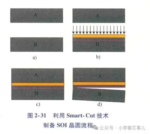
3. “Smart-Cut” Method – The Ultimate Cost-Saving Secret
This is currently the most mainstream and economical technology, a true highlight!
Method:
Hydrogen ions are first implanted into a wafer, like using an “atomic ruler” to draw an invisible “pre-crack line” at a specific depth.
It is then bonded to another wafer with an oxide layer.
By heating, the wafer will magically break precisely along the “pre-crack line”, leaving a perfectly thick top layer of silicon.
Finally, annealing and polishing are performed.
Revolutionary advantages:
High quality: The top layer silicon is of perfect bulk silicon quality.
Material savings: The remaining silicon substrate that is stripped can be recycled, significantly reducing costs!
Precision control: Excellent thickness uniformity.
Currently, the dominant player in this technology is the French company Soitec, from which most high-end SOI wafers in the world originate.