Gallium oxide, as a highly promising #fourth-generation semiconductor material, can withstand ultra-high voltages and is cost-effective. It is widely used in systems such as electric vehicles, rail transit, 5G/6G base stations, smart grids, and aerospace, earning the title of the “star material” for the next generation of high-power electronic devices. However, as an emerging material, the application of gallium oxide still faces many technical bottlenecks that need to be overcome.
Recently, significant progress has been reported in the domestic gallium oxide field.
Fujia Gallium Industry Breaks Through 6-Inch VB Method Gallium Oxide Single Crystal Preparation Technology
On September 15, Hangzhou Fujia Gallium Industry Technology Co., Ltd. (hereinafter referred to as Fujia Gallium) announced a major breakthrough in the field of gallium oxide crystal growth— successfully preparing a 6-inch gallium oxide single crystal ingot for the first time in China using the vertical Bridgman method (VB method), with a crystal height of 30mm, meeting the processing requirements for conductive materials needed for power devices and enabling the complete processing of 6-inch gallium oxide conductive substrates.
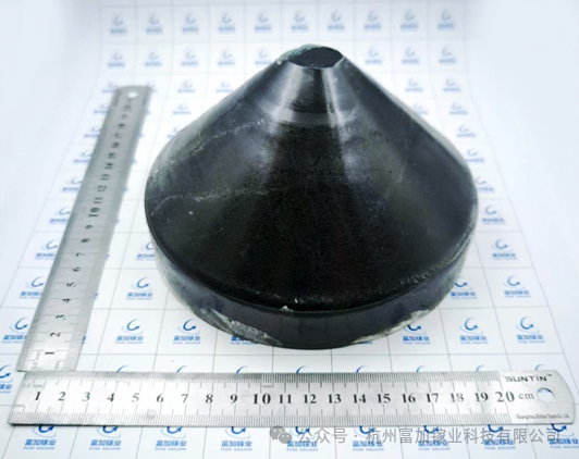
Image Source: Hangzhou Fujia Gallium Industry Technology Co., Ltd.
The image shows the 6-inch VB method gallium oxide single crystal ingot.
Previously, in December 2024, #Fujia Gallium was the first in China to achieve the preparation of 4-inch VB method gallium oxide crystals, and this breakthrough in 6-inch single crystals represents a leap in crystal size.
To date, Fujia Gallium has conducted multiple rounds of 2-6 inch VB method gallium oxide crystal growth, continuously upgrading equipment performance and verifying the stability of growth equipment. The company has launched its own intellectual property rights for VB method gallium oxide crystal growth equipment and supporting growth process packages, accelerating the construction of the industrial ecosystem in the gallium oxide field and promoting the vigorous development of the gallium oxide semiconductor industry.
In the future, Fujia Gallium will continue to adhere to the concept of innovation-driven development and the prosperity of the gallium oxide industry, actively collaborating with universities, research institutions, and upstream and downstream units of the industrial chain to continuously improve equipment and process technology levels, jointly promoting the industrial application of gallium oxide materials.
Su Zhou Nano Institute’s Nano Processing Platform Achieves Progress in β-Ga₂O₃ Vertical Power Devices
Recently, the Nano Processing Platform of the Suzhou Institute of Nano Technology and Nano Bionics, Chinese Academy of Sciences, achieved two important breakthroughs in the field of gallium oxide (β-Ga₂O₃) power devices: for the first time, a multi-fin channel ohmic contact anode β-Ga₂O₃ diode (MFCD) was developed based on the nano processing platform, achieving ultra-low leakage with kilovolt-level breakdown voltage; simultaneously, a high-performance enhanced vertical β-Ga₂O₃ multi-fin transistor was developed, setting a record for the lowest specific on-resistance of 4.3mΩ·cm². These two achievements provide new solutions for high-temperature and high-pressure application scenarios.
 Multi-fin channel diode—breaking the limitations of traditional vertical structures
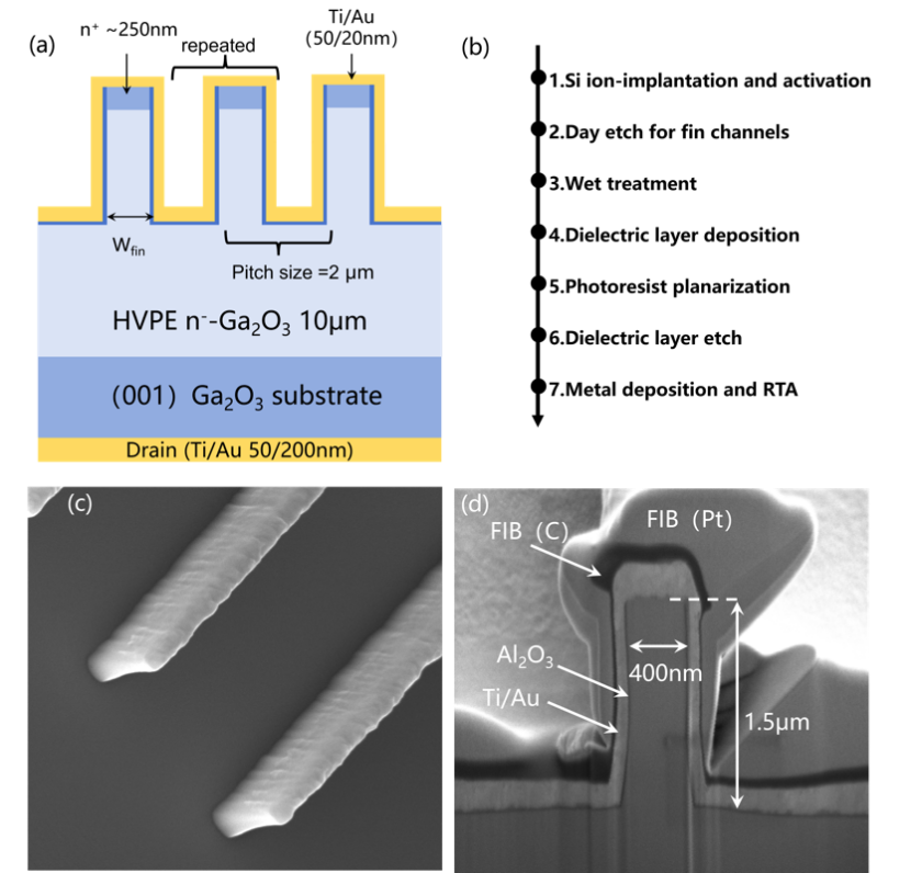
Image Source: Chinese Academy of Sciences Suzhou Nano Institute
Figure (a) Schematic diagram of the multi-fin channel β-Ga₂O₃ diode, (b) Key process steps of the device, (c) Scanning electron microscope (SEM) image after fin dry etching, (d) SEM cross-sectional image of the fin width 400 nm diode
This device replaces the traditional Schottky structure with an innovative ohmic contact anode design, combined with the sidewall self-depletion effect caused by sub-micron fin channels, successfully solving the leakage control problem of wide bandgap semiconductor devices under high electric fields. Without any field plates or passivation layers, the 0.1μm narrow fin device exhibits a breakdown voltage of 1148V, with reverse leakage current stably maintained at a commercial level of 1μA/cm², and no performance degradation observed in a high-temperature environment of 150°C. The introduction of ohmic contact reduces the specific on-resistance to 7mΩ·cm², a 35% reduction compared to similar trench Schottky diodes, and this breakthrough provides new solutions for high-voltage scenarios such as photovoltaic inverters and electric vehicle fast charging stations.
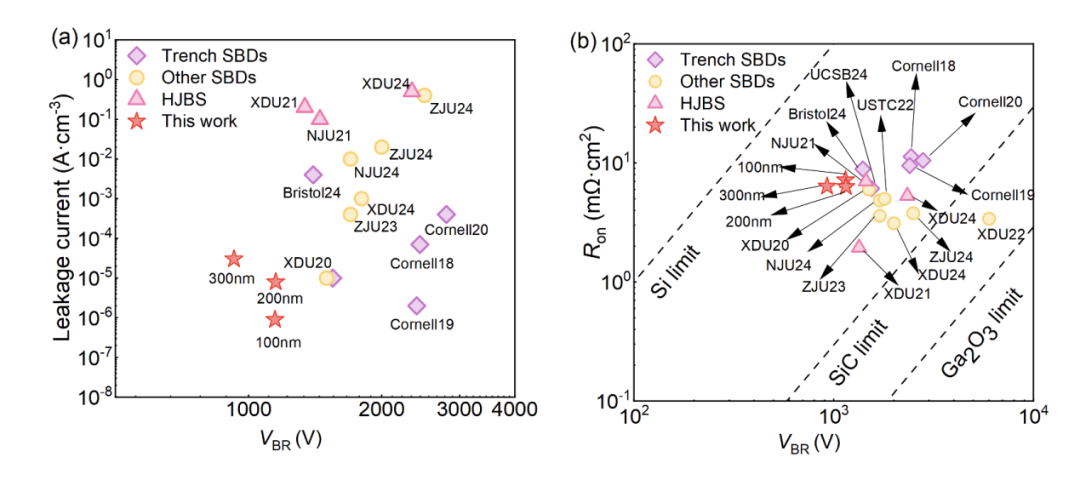
Image Source: Chinese Academy of Sciences Suzhou Nano Institute
Figure (a) Comparison of leakage current and breakdown voltage performance benchmarks of vertical diodes, (b) Comparison of the on-resistance and breakdown voltage performance benchmarks of β-Ga₂O₃ vertical diodes and trench SBDs in this work, as well as reported results in the literature
This achievement was published under the title Kilovolt-Class β-Ga₂O₃ Multi-Fin-Channel Diodes with Ohmic-Contact Anode at the 37th International Symposium on Power Semiconductor Devices and ICs 2025, with the first authors being Guo Gaofu and Zhang Xiaodong from the Suzhou Institute of Nano Technology, Chinese Academy of Sciences, and the corresponding authors being Researcher Zhang Baoshun and Professor Dai Xianqi from Henan Normal University.
 Enhanced vertical transistor—solving the “normally-on” problem
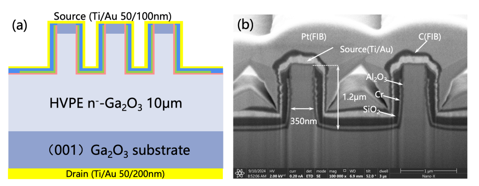
Image Source: Chinese Academy of Sciences Suzhou Nano Institute
Figure (a) Schematic diagram of the multi-fin channel β-Ga₂O₃ FinFET, (b) SEM cross-sectional image of the fin width 300 nm diode
To address the core bottleneck of the lack of p-type doping in gallium oxide materials, the research team simultaneously developed an internationally leading enhanced vertical multi-fin transistor. By employing a dual-gate fin channel geometric confinement technology, reliable normally-off characteristics are achieved without relying on a p-type layer, with a threshold voltage of 0.87V and a switching ratio exceeding 7×10⁶. The innovative use of electron beam lithography and non-metal mask etching technology allows for precise control of fin width at 350nm, combined with dual self-aligned planarization technology to accurately construct the source-drain contact area.
The final device outputs an ultra-high current density of 760A/cm² at a working voltage of 10V, with a specific on-resistance of only 4.3mΩ·cm², while maintaining a breakdown voltage of 975V and an excellent power quality factor (PFOM) of 0.22GW/cm², laying a key technological foundation for the localization of power supply and industrial motor drive chips.
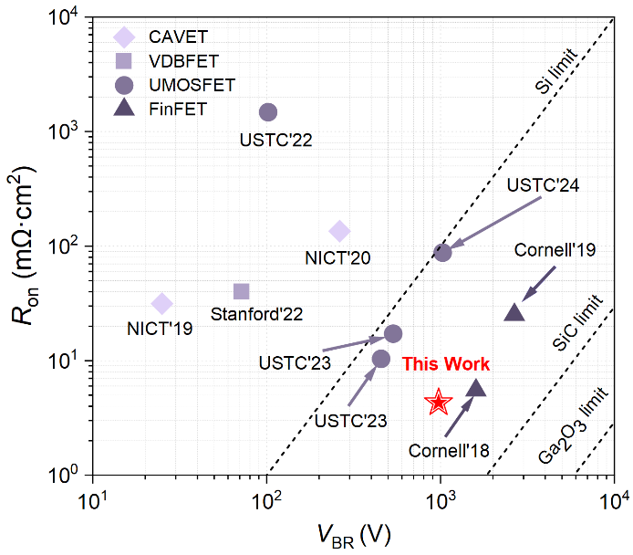
Image Source: Chinese Academy of Sciences Suzhou Nano Institute
Figure Comparison of Vbr and R(on,sp) performance of the latest vertical β-Ga₂O₃ MOSFET devices
This achievement was published under the title 975V/4.3mΩ·cm² Enhancement-mode (001) β-Ga₂O₃ Vertical Multi-fin Power Transistors at the 9th IEEE Electron Devices Technology and Manufacturing Conference 2025, with the first author being Guo Gaofu from the Suzhou Institute of Nano Technology, Chinese Academy of Sciences, and the corresponding authors being Researcher Zhang Baoshun and Professor Dai Xianqi from Henan Normal University.
Gallium Oxide Successfully Partners with the “Thermal King” Diamond
According to China Science News, Academician of the Chinese Academy of Sciences and Professor at Xi’an University of Electronic Science and Technology, Hao Yue’s team, led by Professors Zhang Jincheng and Ning Jing, cleverly introduced graphene as a “translator” to successfully connect gallium oxide with the “thermal king” diamond, solving the heat dissipation problem and allowing chips to operate “coolly”. Relevant research results were recently published in Nature Communications.
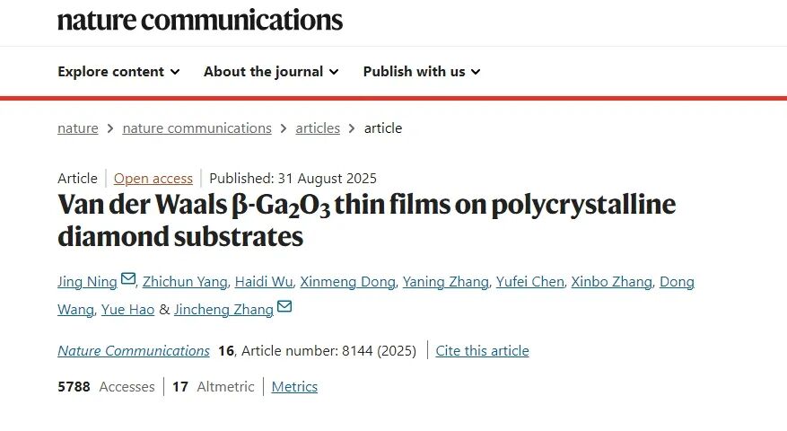
Image Source: Screenshot from Nature Communications article
Although gallium oxide has broad application prospects, it suffers from poor thermal conductivity. It is reported that the thermal conductivity of gallium oxide is only 1/5 that of silicon materials, which can easily lead to device damage and performance degradation. To “cool down” gallium oxide, the research team initially considered using diamond, which has excellent thermal conductivity, but single crystal diamonds are small in size and expensive, making large-scale use difficult. Therefore, the team turned to the more cost-effective “polycrystalline diamond”, but when growing gallium oxide thin films on polycrystalline substrates, the material tends to “grow chaotically” (crystal orientation disorder), resulting in cracks and stress, significantly reducing the heat dissipation effect.
Finally, the team introduced “graphene” as an intermediate buffer layer, which solved the “communication barrier” between the two materials, shielding the roughness of the polycrystalline substrate, allowing the gallium oxide thin film to grow smoothly and with high quality on polycrystalline diamond. The team also achieved stable epitaxy of high-quality gallium oxide thin films through “oxygen-lattice synergistic regulation” technology, which precisely controls the arrangement of oxygen and atoms, thus preventing the material from “growing chaotically” and significantly reducing thermal stress.
Experiments measured that the thermal resistance between gallium oxide and diamond is only 2.82 m²·K/GW—significantly reducing the interfacial thermal resistance to about 1/10 of that of traditional technologies.
This breakthrough is not just a laboratory achievement; it also addresses the “self-heating” pain point of gallium oxide devices, allowing for an efficient “marriage” between high thermal conductivity diamond and gallium oxide, providing a new approach to solving the heating problem of gallium oxide devices and laying the foundation for the development of high-performance, high-reliability electronic devices in the future.
It releases interfacial thermal stress, allowing heat to be efficiently transferred. Experiments measured that the thermal resistance between gallium oxide and diamond is only 2.82 m²·K/GW—significantly reducing the interfacial thermal resistance to about 1/10 of that of traditional technologies.


TrendForce Compound Semiconductor Overview
About TrendForce

TrendForce is a global high-tech industry research organization, with research areas covering memory, AI servers, integrated circuits and semiconductors, wafer foundry, display panels, LEDs, AR/VR, new energy (including solar photovoltaics, energy storage, and batteries), AI robotics, and automotive technology. With years of in-depth research, TrendForce is committed to providing forward-looking industry research reports, industry analysis, project planning assessments, corporate strategic consulting, and brand integration marketing services to government and enterprise clients, making it a trusted decision-making partner in the high-tech field.
