Hello everyone, welcome to <span>LiXin Embedded</span>.
Today, we will discuss JTAG boundary scan. This tool is essential for testing PCB interconnections and internal chip logic, defined in the IEEE 1149.1 standard. If you haven’t read the first two articles in this series, I recommend going back to catch up on the basics of JTAG debugging.
Without further ado, let’s dive into the principles, core components, and practical operations of boundary scan.
The Underlying Logic of Boundary Scan
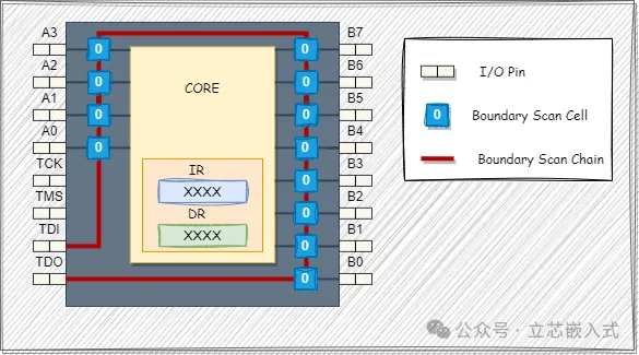
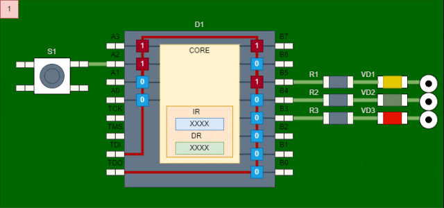
The essence of boundary scan lies in a small component called scan cell. These cells act as “gatekeepers” between the chip pins and internal logic, remaining transparent during normal operation to allow signals to flow. Once in boundary scan mode, they transform to isolate the core logic of the chip from the pins, with signals entirely managed by the JTAG interface.
These scan cells are connected in a Boundary Scan Register (BSR), which is essentially a serial shift register. Through JTAG commands, you can write data into this register, control pin outputs, or read the current state of the pins. In simple terms, boundary scan allows precise control of chip pins via JTAG commands to test whether the connections on the board are reliable or if there are issues with the internal logic of the chip.
Scan Cells: The Soul of Boundary Scan
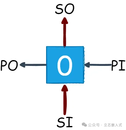
Scan cells are the absolute core of boundary scan, akin to a “Swiss Army knife” for chip testing. Each cell can be flexibly configured to perform various tasks, such as capturing input signals, outputting specified levels, or even acting as a “transparent” entity between pins and logic, doing nothing at all.
Classification of Scan Cells
Based on functionality, scan cells can be roughly classified into the following categories:
- Input Cell: Specifically monitors input signals and pin states.
- Output Cell:
- Output2: Simple and straightforward, only supports two states: 0 or 1, without tri-state logic.
- Output3: More advanced, supports 0, 1, and Hi-Z (high impedance), suitable for complex scenarios.
- Bidirectional Cell: Capable of both input and output, usually supports tri-state logic, flexible like a versatile player.
- Control Cell:
- Control: Responsible for directing other cells, such as switching between input and output modes, acting as the “director”.
- ControlR: Has the added ability to read the state, providing real-time information about the controlled cells.
- Clock Cell: Specifically interacts with the system clock, supports INTEST mode, particularly useful for testing internal logic.
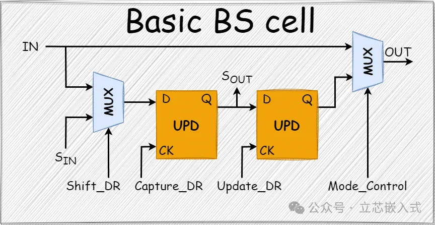
Each scan cell internally consists of a combination of several flip-flops and logic circuits; although small, they are fully equipped. The IEEE 1149.1 standard defines ten types of cell (BC_1 to BC_10), each with its own specialties. For example, BC_1 is versatile and can perform various tasks; BC_4 is optimized for clock pins to reduce signal delay. Want to know the specifics? You need to check the chip’s BSDL file, which details everything clearly.
TIPs
The number of scan cells does not necessarily correspond one-to-one with the number of pins. For example, a bidirectional pin may require three cells: one for input, one for output, and one for state control. In actual design, manufacturers often combine input and output cells into a multifunctional cell, such as BC_7, to save space.
Boundary Scan Register (BSR): Data Transfer Station
The BSR is the “data highway” that connects all scan cells. Through JTAG’s TDI (Test Data Input) and TDO (Test Data Output), you can shift data into or out of the BSR. The size and structure of the BSR depend on the specific design of the chip, which manufacturers will detail in the BSDL file.
For example, in the case of STM32F411, the BSDL file might tell you:
- The BSR contains a total of 405 cells (bits).
- A pin may correspond to multiple cells; for instance, pin PE2 has input, output, and control cells, each responsible for different functions.
Before testing, you need to clarify the length and order of the BSR; otherwise, if the data is written incorrectly, the test results will be a mess.
Boundary Scan Instruction Set: The Baton of Testing
The IEEE 1149.1 standard defines a set of instructions that control the behavior of boundary scan. Here are a few commonly used ones that embedded engineers must be familiar with:
SAMPLE Instruction
This instruction is like a covert operation, quietly capturing the current state of the pins and storing it in the BSR, then outputting it through TDO. The key is that the chip operates normally without being affected, making it suitable for real-time signal monitoring. For example, if you want to know what a certain GPIO pin is doing, you can use SAMPLE to find out immediately.
PRELOAD Instruction
PRELOAD is the instruction for “preloading ammunition” into the BSR. You can use it to write specified data into the scan cells, preparing for subsequent tests. Note that at this point, the data is only loaded into the BSR and does not affect the pins; the LED will not light up, and the output will not change.

SAMPLE/PRELOAD Combination
As the name suggests, this instruction combines SAMPLE and PRELOAD. It first captures the pin state and stores it in the BSR, then allows you to write new data into it. This is usually the first step in boundary scan testing, paving the way for subsequent operations.
EXTEST Instruction
EXTEST is the ace up your sleeve for testing external circuits. When entering this mode, the internal logic of the chip is isolated, and the pins are entirely controlled by the BSR. You can output the preloaded data through EXTEST to the pins, checking for issues like short circuits or open circuits on the board. EXTEST is definitely a powerful tool for verifying board quality on the production line.
INTEST Instruction
INTEST, on the other hand, focuses on testing the internal logic of the chip. The BSR controls the signal input to the core logic, checking for any faults within the chip. However, this mode is not used frequently, mainly for verifying chip models or identifying obvious internal defects.
Other Instructions
- BYPASS: Directly connects TDI to TDO, doing nothing, just passing through.
- CLAMP: Fixes pin outputs while following the BYPASS path.
- HIGHZ: Sets all pins to high impedance, suitable for isolation testing.
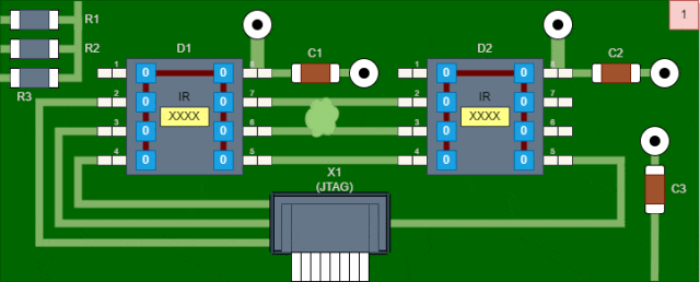
Practical Case: Using Boundary Scan to Identify Board Issues
After discussing the theory, let’s get practical. Suppose you have a board with two chips, D1 and D2, where pins 5, 6, and 7 of D1 are connected to pins 2, 3, and 4 of D2. Now you want to use JTAG to check if these connections are problematic, but unfortunately, there is a solder bridge between pins 6 and 7 of D1 and pins 2 and 3 of D2, causing a short circuit.
Testing Steps
- Use PRELOAD to load data into D1: Write a test pattern into D1’s BSR, such as 0b0101010000.
- Use EXTEST to output signals: Have D1’s pins output signals according to the pattern.
- Use SAMPLE to read D2’s state: Read the states of D2’s pins 2, 3, and 4, expecting 0b00001010 (corresponding to D1’s output). However, if you actually read 0b00001000, it indicates that there is an issue with the connection from D1:7 to D2:2.
Analysis
This test directly detected the solder bridge. D2’s pin 2 was pulled low due to the short circuit, resulting in an incorrect signal. Next, grab the soldering iron and clean up the solder bridge, and the problem is solved!
Final Thoughts
At first glance, JTAG boundary scan seems complex and overwhelming, but once understood, it becomes a lifesaver for testing boards and chips. From scan cells to BSR, and through various instructions, each step is filled with the wisdom of engineers. To quote an old saying, the more you learn, the more you realize how little you know; this technology is deep and unfathomable, and every pitfall teaches you something new.
Do you have any experiences with JTAG or pitfalls you’ve encountered? Feel free to leave a comment! In the next issue, we will continue discussing the intricacies of BSDL files, so stay tuned!