
Click the blue text
Follow us
1. Introduction to SPI
SPI (Serial Peripheral Interface) is a synchronous, serial, full-duplex communication interface commonly used for data exchange between microcontrollers, sensors, memory, and other external devices. Examples include: EEPROM, RTC (Real-Time Clock), ADC (Analog-to-Digital Converter), DAC (Digital-to-Analog Converter), LCD, audio ICs, temperature and pressure sensors, MMC or SD cards, etc.
2. SPI Communication Structure
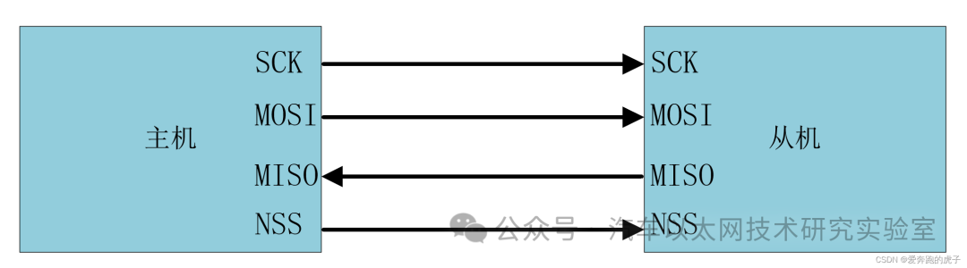
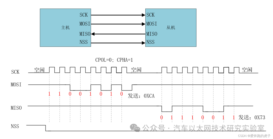
SPI is a synchronous data bus, which requires a clock signal for synchronous communication. This means that SPI uses separate data lines and a single clock signal to ensure perfect synchronization between the sender and receiver. The communication structure is shown in the figure below:
-
SCK: The clock signal for SPI communication, generated by the master, with the slave receiving the clock. There is only one master in the SPI communication structure, but there can be multiple slaves.
-
MOSI: (Master Output Slave Input) The master outputs data to the slave.
-
MISO: (Master Input Slave Output) The master receives data from the slave.
-
NSS: (Negative Slave Select) The slave select signal, active low (sent from the master to the slave).
3. Multi-Slave Mode
-
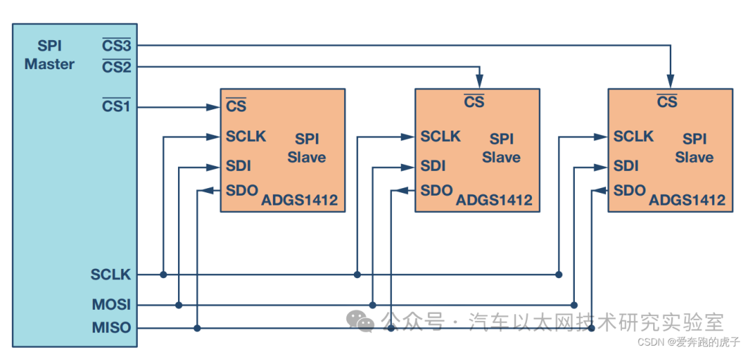
Conventional Mode: The master needs to provide a separate chip select signal for each slave. Once the master pulls the chip select signal low, the clock and data on the MOSI or MISO lines can be used for the selected slave. If multiple chip select signals are pulled low, the data on the MISO line will be corrupted because the master cannot identify which slave is transmitting data.
-
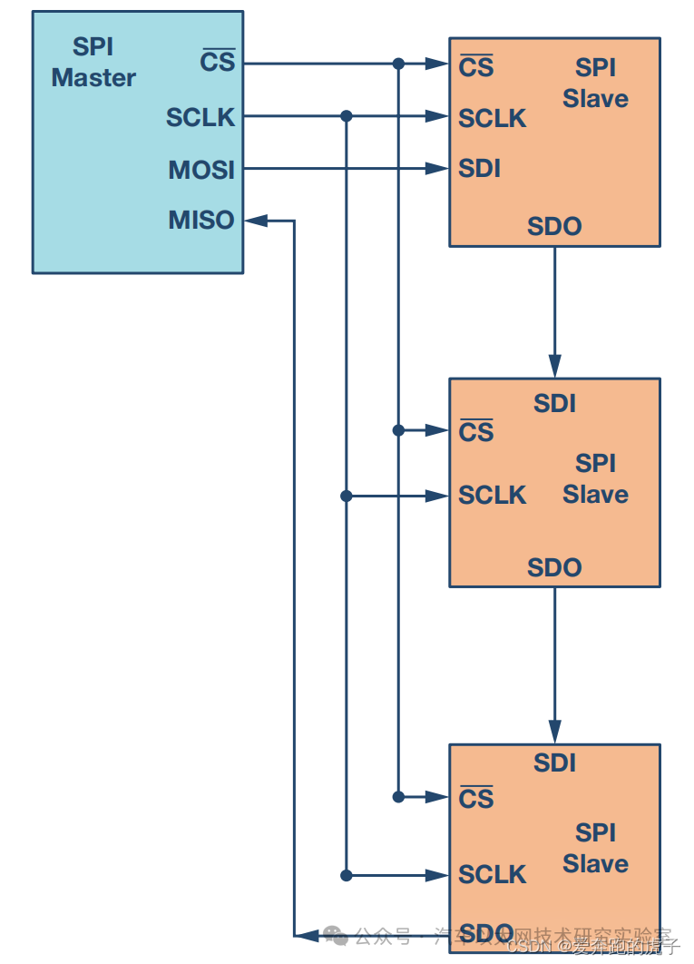
Daisy Chain Mode: All slave chip select signals are connected together, and data propagates from one slave to the next. All slaves receive the same SPI clock simultaneously. Data from the master is sent directly to the first slave, which then provides the data to the next slave, and so on.
4. Clock Polarity (CPOL) and Clock Phase (CPHA)
In SPI, the master needs to configure the clock polarity and clock phase.
-
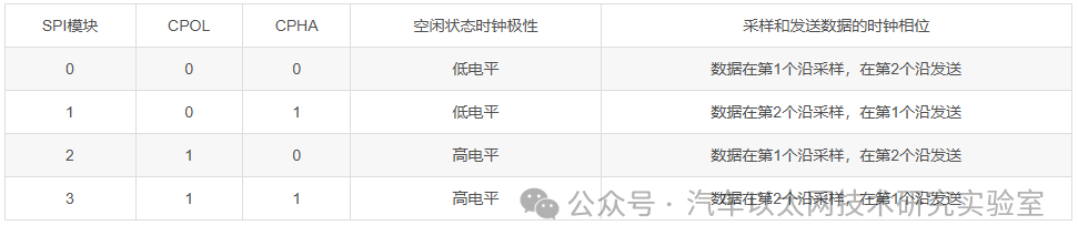
During idle state, the CPOL bit sets the polarity of the clock signal. The idle state refers to the period when CS is high before transitioning to low, and when the transmission ends with CS low before transitioning to high. CPOL = 0: Clock is low during idle; CPHA = 1: Clock is high during idle.
-
CPHA bit selects the clock phase. Depending on the state of the CPHA bit, data is sampled or sent on the rising or falling edge of the clock. CPHA = 0: Sample on the first edge of the clock signal SCK; CPHA = 1: Sample on the second edge of the clock signal SCK.
-
The master must select the clock polarity and clock phase according to the requirements of the slave. Based on the selection of CPOL and CPHA bits, four SPI modes are available.
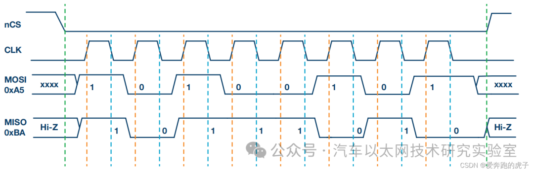
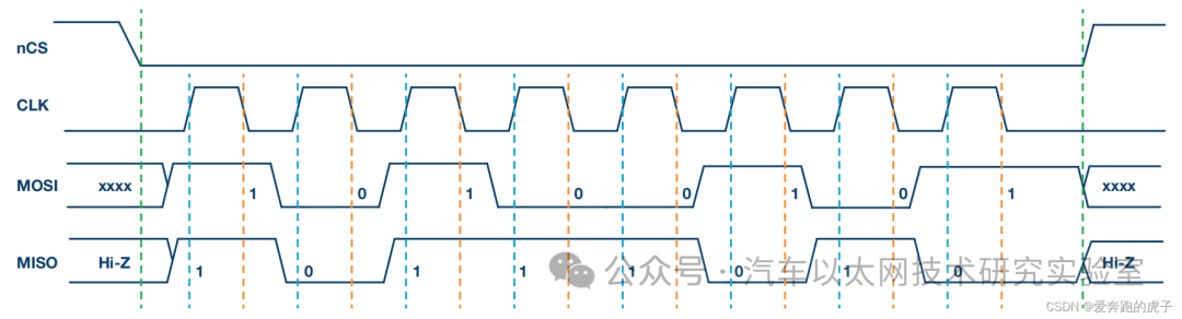
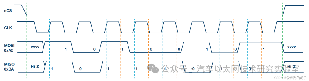
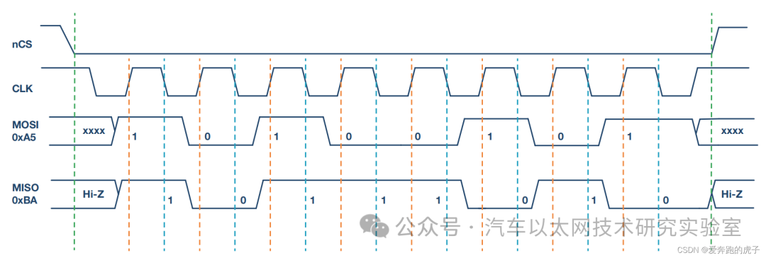
The four transmission modes are shown below, with the start and end of transmission indicated by green dashed lines, the sampling edge indicated by orange dashed lines, and the sending edge indicated by blue dashed lines.
-
SPI Mode 0, CPOL = 0, CPHA = 0: CLK idle state = low, data is sent on the falling edge and sampled on the rising edge.
-
SPI Mode 1, CPOL = 0, CPHA = 1: CLK idle state = low, data is sent on the rising edge and sampled on the falling edge.
-
SPI Mode 2, CPOL = 1, CPHA = 0: CLK idle state = high, data is sent on the rising edge and sampled on the falling edge.
-
SPI Mode 3, CPOL = 1, CPHA = 1: CLK idle state = high, data is sent on the falling edge and sampled on the rising edge.
5. SPI Communication Process
-
The master pulls the NSS signal low to select the corresponding slave before accessing it; when the master wants to end the communication, it pulls the NSS signal high again.
-
The master sends the SCLK clock signal.
-
The master sends data bit by bit to the slave via MOSI according to the configured clock polarity and clock phase.
-
The slave receives data bit by bit at the corresponding position based on the clock polarity and clock phase configured by the master.
6. Implementing the SPI Master Send Program
6.1 Waveform Analysis
-
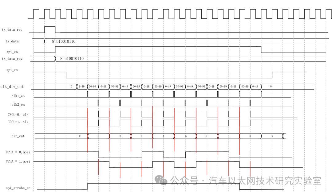
When no data is being sent, spi_en is low. When there is a request to send data, the spi_en signal is pulled high and the data to be sent is buffered.
-
Then, the cs signal is pulled low to start the clock counting.
-
Every half cycle, the first clock edge signal is pulled high, and when a full cycle is counted, the second clock edge signal is pulled high.
-
If CPOL=0, the clock is low during idle, and the first clock edge is the rising edge. If CPOL=1, it is the opposite.
-
Every time the first clock edge arrives, the bit counter for the sent bits increments.
-
If CPHA=0, data is sampled on the first clock edge (rising edge), as shown by the red line above. For example, if the data sent is 10010110, the sampled data will also be 10010110.
-
If CPHA=1, data is sampled on the second clock edge (falling edge), as shown by the red line below. For example, if the data sent is 10010110, the sampled data will also be 10010110.
6.2 Verilog Code
-
`timescale 1ns/1ns
-
module spi_master_tx#
-
(
-
parameter SYS_CLK_FREQ = 50000000, // Input clock frequency 50M
-
parameter SPI_CLK_FREQ = 500000, // Output SPI clock 500K
-
parameter CPOL = 1’b0, // Clock polarity set to 0
-
parameter CPHA = 1’b0 // Clock phase set to 0
-
)
-
(
-
input sys_clk , // Input system clock
-
input rst_n , // System reset
-
input spi_tx_req , // Request to send data
-
input [7:0] spi_tx_data , // Data to be sent
-
output reg spi_cs , // CS chip select signal
-
output spi_clk , // SPI clock sent by the master
-
output spi_busy, // SPI busy signal
-
output spi_mosi // MOSI
-
);
-
localparam [9:0] spi_clk_cnt_max = SYS_CLK_FREQ / SPI_CLK_FREQ; // Maximum count for one SPI clock
-
localparam [9:0] spi_clk_cnt_max_div2 = spi_clk_cnt_max/2; // Maximum count for half a clock cycle
-
reg [9:0] clk_div_cnt ; // SPI clock counter
-
reg spi_en ; // SPI send enable
-
reg [7:0] spi_tx_data_reg ; // Buffer for data to be sent
-
reg clk1_en ; // First clock edge
-
reg clk2_en ; // Second clock edge
-
reg spi_clk_temp ; // SPI clock
-
reg [3:0] tx_cnt ; // Bit counter for sent data
-
reg spi_strobe_en ; // Valid range for SPI send data enable
-
wire strobe ; // SPI send data enable signal
-
// If clock polarity = 1, invert the clock signal
-
assign spi_clk = (CPOL == 1’b1)? ~spi_clk_temp : spi_clk_temp;
-
// Send high bit data first
-
assign spi_mosi = spi_tx_data_reg[7];
-
// If clock phase = 1, sample data on the second clock edge, send data on the first clock edge
-
assign strobe = (CPHA == 1’b1)? clk1_en&spi_strobe_en : clk2_en&spi_strobe_en;
-
// SPI busy signal equals SPI send enable signal
-
assign spi_busy = spi_en;
-
// Wait for upstream to provide send request and send data. After sending 8 bits, the transmission is complete.
-
always @(posedge sys_clk or negedge rst_n) begin
-
if((rst_n == 1’b0) || (clk1_en == 1’b1 && tx_cnt == 4’d8)) begin
-
spi_en <= 1’b0;
-
spi_tx_data_reg <= ‘d0;
-
end
-
else if((spi_tx_req == 1’b1) && (spi_en == 1’b0))begin
-
spi_en <= 1’b1;
-
spi_tx_data_reg <= spi_tx_data;
-
end
-
else if(spi_en == 1’b1 && strobe)
-
spi_tx_data_reg <= {spi_tx_data_reg[6:0],1’b0};
-
else
-
spi_tx_data_reg <= spi_tx_data_reg;
-
end
-
// Pull down cs signal before sending starts
-
always @(posedge sys_clk or negedge rst_n) begin
-
if(rst_n == 1’b0)
-
spi_cs <= 1’b1;
-
else if(spi_en == 1’b1)
-
spi_cs <= 1’b0;
-
else
-
spi_cs <= 1’b1;
-
end
-
// When the clock counter counts to half, pull high the first clock edge signal, and when a full clock cycle is counted, pull high the second clock signal
-
always @(posedge sys_clk or negedge rst_n) begin
-
if((rst_n == 1’b0) || (spi_cs == 1’b1))begin
-
clk_div_cnt <= 0;
-
clk1_en <= 1’b0;
-
clk2_en <= 1’b0;
-
end
-
else if(clk_div_cnt == spi_clk_cnt_max – 1)begin
-
clk_div_cnt <= 0;
-
clk2_en <= 1’b1;
-
end
-
else if(clk_div_cnt == spi_clk_cnt_max_div2 – 1)begin
-
clk1_en <= 1’b1;
-
clk_div_cnt <= clk_div_cnt + 1’b1;
-
end
-
else begin
-
clk_div_cnt <= clk_div_cnt + 1’b1;
-
clk1_en <= 1’b0;
-
clk2_en <= 1’b0;
-
end
-
end
-
// Every time the first clock edge comes, it indicates that a number has been sent
-
always @(posedge sys_clk or negedge rst_n) begin
-
if((rst_n == 1’b0)||(spi_en == 1’b0))
-
tx_cnt <= ‘d0;
-
else if(clk1_en == 1’b1)
-
tx_cnt <= tx_cnt + 1’b1;
-
else
-
tx_cnt <= tx_cnt;
-
end
-
always @(posedge sys_clk or negedge rst_n) begin
-
if(rst_n == 1’b0)
-
spi_strobe_en <= 1’b0;
-
else if(tx_cnt < 4’d8)
-
if(clk1_en == 1’b1 )
-
spi_strobe_en <= 1’b1;
-
else
-
spi_strobe_en <= spi_strobe_en;
-
else
-
spi_strobe_en <= 1’b0;
-
end
-
always @(posedge sys_clk or negedge rst_n) begin
-
if(rst_n == 1’b0)
-
spi_clk_temp <= 1’b0;
-
else if(clk2_en == 1’b1)
-
spi_clk_temp <= 1’b0;
-
else if((clk1_en == 1’b1)&&(tx_cnt <4’d8))
-
spi_clk_temp <= 1’b1;
-
else
-
spi_clk_temp <= spi_clk_temp;
-
end
-
endmodule
6.3 Data Sending Control Module
A simple data sending control module is set up, where the data sent starts from 1 and increments. The code is as follows:
-
`timescale 1ns / 1ps
-
module spi_top
-
(
-
input sys_clk , // Input clock
-
input rst_n , // System reset
-
output spi_clk , // SPI send clock
-
output spi_mosi // SPI send data
-
);
-
wire spi_cs ;
-
wire spi_busy ; // SPI busy signal
-
reg spi_tx_req ; // SPI send req signal, pulled high when there is a sending demand
-
reg [7:0] spi_tx_data ; // Data to be sent storage
-
reg [1:0] state ; // State machine
-
// SPI send state machine
-
always @(posedge sys_clk) begin
-
if(!rst_n) begin
-
spi_tx_req <= 1’b0;
-
spi_tx_data <= 8’d0;
-
state <= 2’d0;
-
end
-
else begin
-
case(state)
-
0:if(!spi_busy)begin // Start transmission when the bus is not busy
-
spi_tx_req <= 1’b1; // Pull req signal high to start transmission
-
spi_tx_data <= spi_tx_data + 1’b1; // Test data
-
state <= 2’d1;
-
end
-
1:if(spi_busy)begin // If the SPI bus is busy, clear spi_tx_req
-
spi_tx_req <= 1’b0;
-
state <= 2’d0;
-
end
-
default:state <= 2’d0;
-
endcase
-
end
-
end
-
// Instantiate SPI Master transmitter
-
spi_master_tx#(
-
.SYS_CLK_FREQ ( 50000000 ),
-
.SPI_CLK_FREQ ( 500000 ),
-
.CPOL ( 1’b0 ),
-
.CPHA ( 1’b0 )
-
)u_spi_master_tx(
-
.sys_clk ( sys_clk ),
-
.rst_n ( rst_n ),
-
.spi_tx_req ( spi_tx_req ),
-
.spi_tx_data ( spi_tx_data ),
-
.spi_cs ( spi_cs ),
-
.spi_clk ( spi_clk ),
-
.spi_busy ( spi_busy ),
-
.spi_mosi ( spi_mosi )
-
);
-
endmodule
6.4 Simulation Code Writing and Simulation Result Analysis
The tb code is as follows:
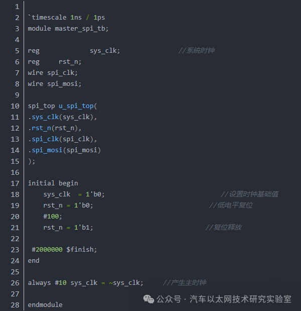
Set CPOL=0, CPHA=0 to observe the simulation results. We randomly select a data point, for example, sending 8’d37, the result is as follows:
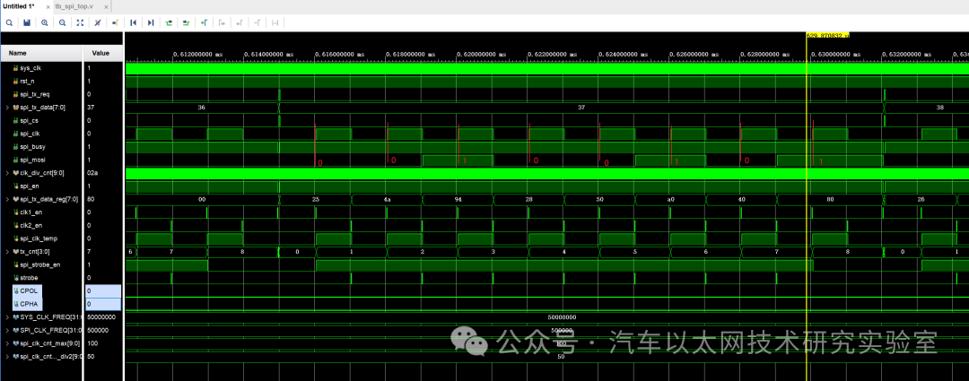
8’d37 in binary is 00100101, so the collected data on the rising edge of the clock is also 00100101, which is correct.
Now modify CPOL=0, CPHA=1 to observe the same result, as shown below:
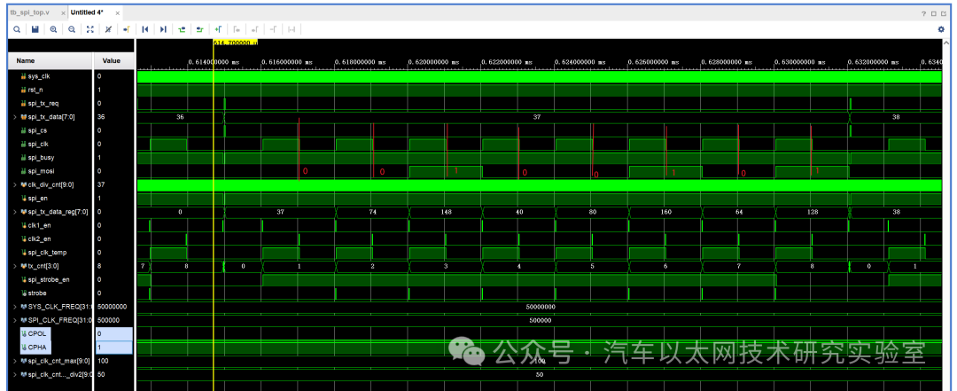
The collected data is on the falling edge of the clock, and the collected data is also 00100101, which is correct.
7. Verilog Implementation of SPI Slave Receive Program
7.1 Waveform Analysis
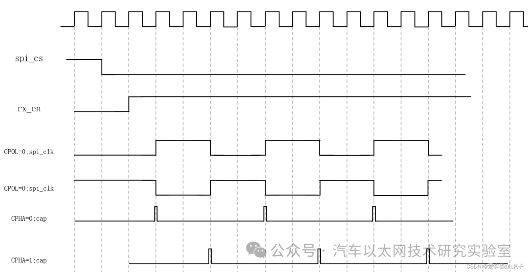
-
The receiver first checks if the cs line is pulled low. If it is low, it enters the receiving state and pulls rx_en high.
-
Then, based on the values of CPOL and CPHA, it finds the edge of the signal to sample.
-
Each time a sampling edge arrives, it samples the data and performs serial-to-parallel conversion.
7.2 Verilog Code
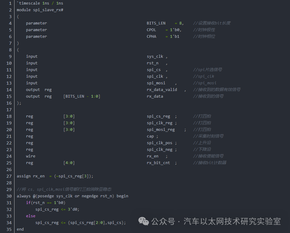
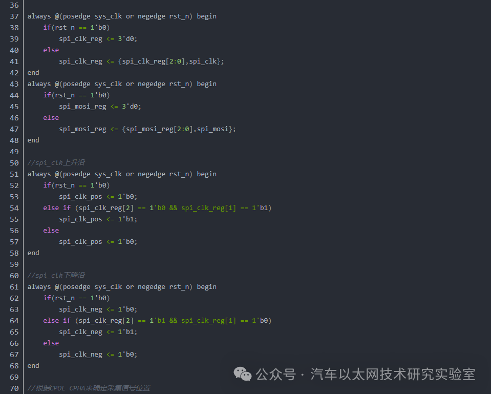
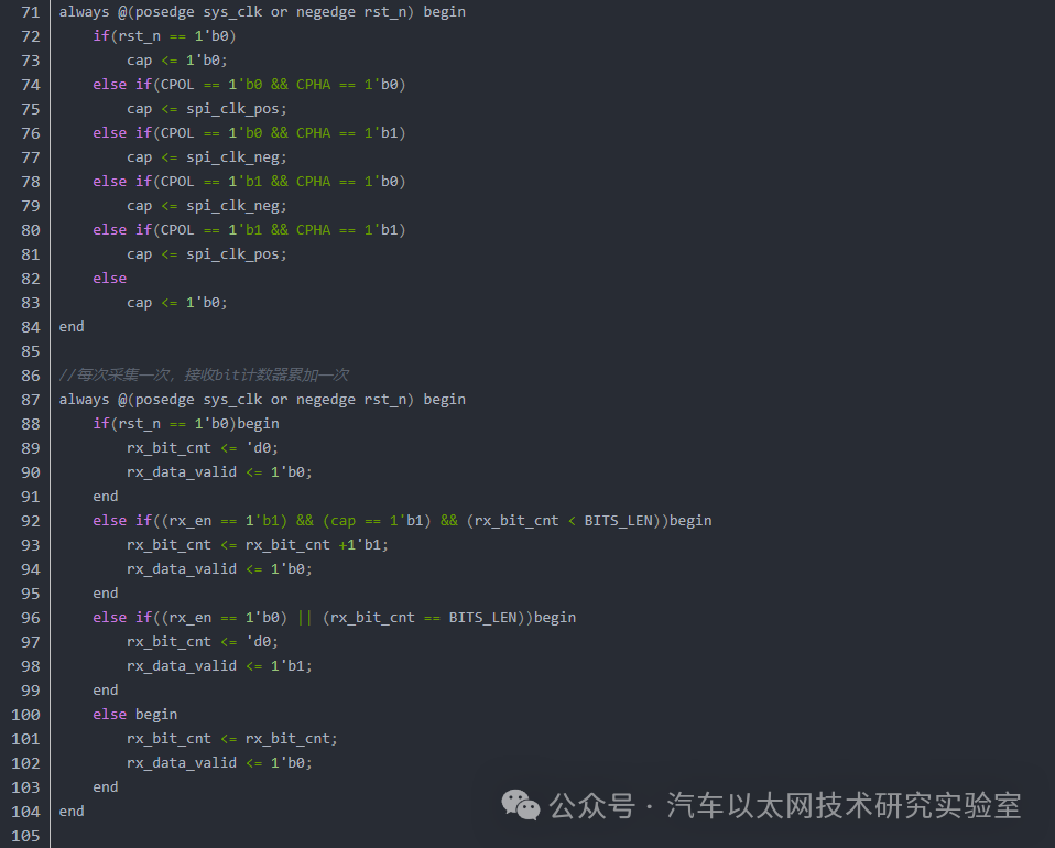
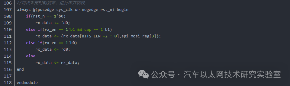
7.3 Simulation Code and Simulation Result Analysis
The tb file is written as follows:
-
`timescale 1ns / 1ps
-
module tb_spi_slave_rtx();
-
localparam BYTES = 8;
-
localparam TCNT = BYTES*8*2-1;
-
localparam CPOL = 1;
-
localparam CPHA = 1;
-
reg I_clk; // System clock
-
reg [7:0] i; // Counter for generating SPI clock count
-
reg I_rstn; // System reset
-
reg I_spi_clk; // SPI clock
-
reg I_spi_ss; // SPI Slave select signal
-
reg [3:0] bit_cnt; // Bit counter
-
reg [7:0] spi_tx_buf; // Send buffer (shift register)
-
reg [7:0] spi_tx_buf_r; // Send buffer for generating test data
-
reg first_data_flag; // Whether to change data on one clock
-
wire O_spi_rvalid; // SPI data receive valid, when this signal is valid, it indicates that valid data has been received
-
wire [7:0] O_spi_rdata; // SPI read data
-
wire I_spi_rx; // SPI data bus
-
// The tb simulates the SPI test data received at I_spi_rx
-
assign I_spi_rx = spi_tx_buf[7];
-
// Instantiate SPI receive module
-
spi_slave_rx#(
-
.BITS_LEN ( 8 ),
-
.CPOL ( CPOL ),
-
.CPHA ( CPHA )
-
)u_spi_slave_rx(
-
.sys_clk ( I_clk ),
-
.rst_n ( I_rstn ),
-
.spi_cs ( I_spi_ss ),
-
.spi_clk ( I_spi_clk ),
-
.spi_mosi ( I_spi_rx ),
-
.rx_data_valid ( O_spi_rvalid ),
-
.rx_data ( O_spi_rdata )
-
);
-
initial begin
-
I_clk = 1’b0;
-
I_rstn = 1’b0;
-
#100;
-
I_rstn = 1’b1;
-
end
-
always #10 I_clk = ~I_clk; // Clock signal toggles to generate system clock
-
initial begin
-
#100;
-
i = 0;
-
forever begin
-
I_spi_clk = CPOL; // Set clock polarity
-
I_spi_ss = 1; // Set SPI SS control signal
-
#2000;
-
I_spi_ss = 0;
-
for(i=0;i<TCNT;i=i+1) #1000 I_spi_clk = ~ I_spi_clk; // Generate SPI clock
-
#2000;
-
I_spi_ss = 1;
-
end
-
end
-
initial begin
-
#100;
-
bit_cnt = 0;
-
first_data_flag =0;
-
spi_tx_buf[7:0] = 8’ha0;
-
spi_tx_buf_r[7:0] = 8’ha0;
-
forever begin
-
// SPI SS control is used to enable transmission
-
wait(I_spi_ss);// SPI SS
-
bit_cnt = 0;
-
spi_tx_buf[7:0] = 8’ha0;
-
spi_tx_buf_r[7:0] = 8’ha0;
-
if((CPHA == 1 && CPOL ==0)||(CPHA == 1 && CPOL ==1))// The case where the first clock edge changes the data
-
first_data_flag = 1; // Set first_data_flag=1 to skip the first edge in the following sending sequence
-
// Start data transmission when SS is low
-
wait(!I_spi_ss);
-
while(!I_spi_ss)begin
-
// CPOL=0 CPHA=0 default SCLK is low, for the sender, the first bit data is placed on the bus in advance
-
if(CPHA == 0 && CPOL ==0)begin
-
@(negedge I_spi_clk) begin // Update the bit to be sent on the falling edge of each clock
-
if(bit_cnt == 7)begin// During continuous sending, after sending 8 bits, update the data
-
bit_cnt = 0;
-
spi_tx_buf_r = spi_tx_buf_r + 1’b1;// Generate new test data
-
spi_tx_buf = spi_tx_buf_r;// Update the sending register
-
end
-
else begin
-
spi_tx_buf = {spi_tx_buf[6:0],1’b0};// Data shifts, update data
-
bit_cnt = bit_cnt + 1’b1;// SPI send bit counter
-
end
-
end
-
end
-
// CPHA=0 CPOL=1 default SCLK is high, for the sender, the first bit data is placed on the bus in advance
-
if(CPHA == 0 && CPOL ==1)begin
-
@(posedge I_spi_clk) begin // Update the bit to be sent on the rising edge of each clock
-
if(bit_cnt == 7)begin // During continuous sending, after sending 8 bits, update the data
-
bit_cnt = 0;
-
spi_tx_buf_r = spi_tx_buf_r + 1’b1;// Generate new test data
-
spi_tx_buf = spi_tx_buf_r; // Update the sending register
-
end
-
else begin
-
spi_tx_buf = {spi_tx_buf[6:0],1’b0};// Data shifts, update data
-
bit_cnt = bit_cnt + 1’b1;// SPI send bit counter
-
end
-
end
-
end
-
// CPHA=1 CPOL=0 default SCLK is low, for the sender, the first SCLK transition updates
-
if(CPHA == 1 && CPOL ==0)begin
-
@(posedge I_spi_clk) begin
-
if(first_data_flag == 1’b1)begin // On the first clock edge, since the first data to be sent has already been initialized, skip the first transition edge
-
first_data_flag = 0;
-
//spi_tx_buf[7:0] = 8’ha0;// The first data to be sent can also be initialized on the first transition edge
-
end
-
else begin
-
if(bit_cnt == 7)begin
-
bit_cnt = 0;
-
spi_tx_buf_r = spi_tx_buf_r + 1’b1;// Generate new test data
-
spi_tx_buf = spi_tx_buf_r;// Update the sending register
-
end
-
else begin
-
spi_tx_buf = {spi_tx_buf[6:0],1’b0}; // Data shifts, update data
-
bit_cnt = bit_cnt + 1’b1;// SPI send bit counter
-
end
-
end
-
end
-
end
-
// CPHA=1 CPOL=1 default SCLK is high, for the sender, the first SCLK transition updates
-
if(CPHA == 1 && CPOL==1)begin
-
@(negedge I_spi_clk) begin
-
if(first_data_flag == 1’b1)begin // On the first clock edge, since the first data to be sent has already been initialized, skip the first transition edge
-
first_data_flag = 0;
-
//spi_tx_buf[7:0] = 8’ha0;// The first data to be sent can also be initialized on the first transition edge
-
end
-
else begin
-
if(bit_cnt == 7)begin
-
bit_cnt = 0;
-
spi_tx_buf_r = spi_tx_buf_r + 1’b1;// Generate new test data
-
spi_tx_buf = spi_tx_buf_r;// Update the sending register
-
end
-
else begin
-
spi_tx_buf = {spi_tx_buf[6:0],1’b0};// Data shifts, update data
-
bit_cnt = bit_cnt + 1’b1;// SPI send bit counter
-
end
-
end
-
end
-
end
-
end
-
end
-
end
-
endmodule
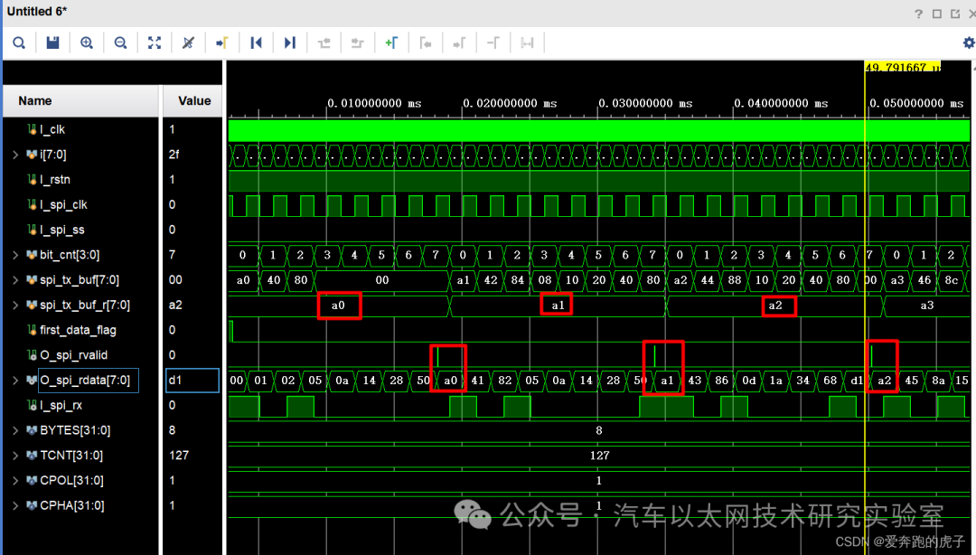
The test results are shown in the figure below, where the upstream sends data a0, and the received module also receives a0.
8. SPI Loopback Test
8.1 Top-Level Code
Connect the SPI sender and SPI receiver together, and simulate sending data through the top-level.
Top-level code:
-
`timescale 1ns / 1ps
-
module spi_top
-
(
-
input sys_clk , // Input clock
-
input rst_n , // System reset
-
input spi_clk_in ,
-
input spi_miso ,
-
output spi_clk , // SPI send clock
-
output spi_mosi // SPI send data
-
);
-
reg spi_cs ;
-
wire spi_busy ; // SPI busy signal
-
reg spi_tx_req ; // SPI send req signal, pulled high when there is a sending demand
-
reg [7:0] spi_tx_data ; // Data to be sent storage
-
reg [1:0] state ; // State machine
-
reg [10:0] delay_cnt ;
-
wire rx_data_valid ;
-
wire [7:0] rx_data ;
-
always @(posedge sys_clk or negedge rst_n) begin
-
if(rst_n == 1’b0)
-
delay_cnt <= ‘d0;
-
else if(delay_cnt[10] == 1’b1)
-
delay_cnt <= ‘d0;
-
else
-
delay_cnt <= delay_cnt +1’b1;
-
end
-
// SPI send state machine
-
always @(posedge sys_clk) begin
-
if(!rst_n) begin
-
spi_tx_req <= 1’b0;
-
spi_tx_data <= 8’d0;
-
state <= 2’d0;
-
spi_cs <= 1’b1;
-
end
-
else begin
-
case(state)
-
0:if((delay_cnt[10]==1’b1) &&(spi_busy == 1’b0))begin
-
spi_cs <= 1’b1;
-
state <= 2’d1;
-
end
-
1:if((delay_cnt[10]==1’b1) &&(spi_busy == 1’b0))begin
-
spi_cs <= 1’b0;
-
state <= 2’d2;
-
end
-
2:if((delay_cnt[10]==1’b1) &&(spi_busy == 1’b0))begin // Start transmission when the bus is not busy
-
spi_tx_req <= 1’b1; // Pull req signal high to start transmission
-
spi_tx_data <= spi_tx_data + 1’b1; // Test data
-
state <= 2’d3;
-
end
-
3:if(spi_busy)begin // If the SPI bus is busy, clear spi_tx_req
-
spi_tx_req <= 1’b0;
-
state <= 2’d0;
-
end
-
default:state <= 2’d0;
-
endcase
-
end
-
end
-
// Instantiate SPI Master transmitter
-
spi_master_tx#(
-
.SYS_CLK_FREQ ( 50000000 ),
-
.SPI_CLK_FREQ ( 500000 ),
-
.CPOL ( 1’b0 ),
-
.CPHA ( 1’b1 )
-
)u_spi_master_tx(
-
.sys_clk ( sys_clk ),
-
.rst_n ( rst_n ),
-
.spi_tx_req ( spi_tx_req ),
-
.spi_tx_data ( spi_tx_data ),
-
.spi_cs ( ),
-
.spi_clk ( spi_clk ),
-
.spi_busy ( spi_busy ),
-
.spi_mosi ( spi_mosi )
-
);
-
spi_slave_rx#(
-
.BITS_LEN ( 8 ),
-
.CPOL ( 1’b0 ),
-
.CPHA ( 1’b1 )
-
)u_spi_slave_rx(
-
.sys_clk ( sys_clk ),
-
.rst_n ( rst_n ),
-
.spi_cs ( spi_cs ),
-
.spi_clk ( spi_clk_in ),
-
.spi_mosi ( spi_miso ),
-
.rx_data_valid ( rx_data_valid ),
-
.rx_data ( rx_data )
-
);
-
ila_0 u_ila (
-
.clk(sys_clk), // input wire clk
-
.probe0(rx_data_valid), // input wire [0:0] probe0
-
.probe1(rx_data) // input wire [7:0] probe1
-
);
-
endmodule
8.2 Simulation Code and Simulation Result Analysis
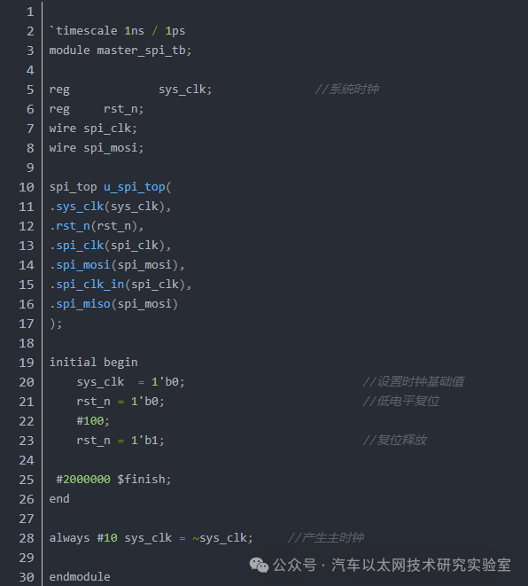
The simulation results are as follows:
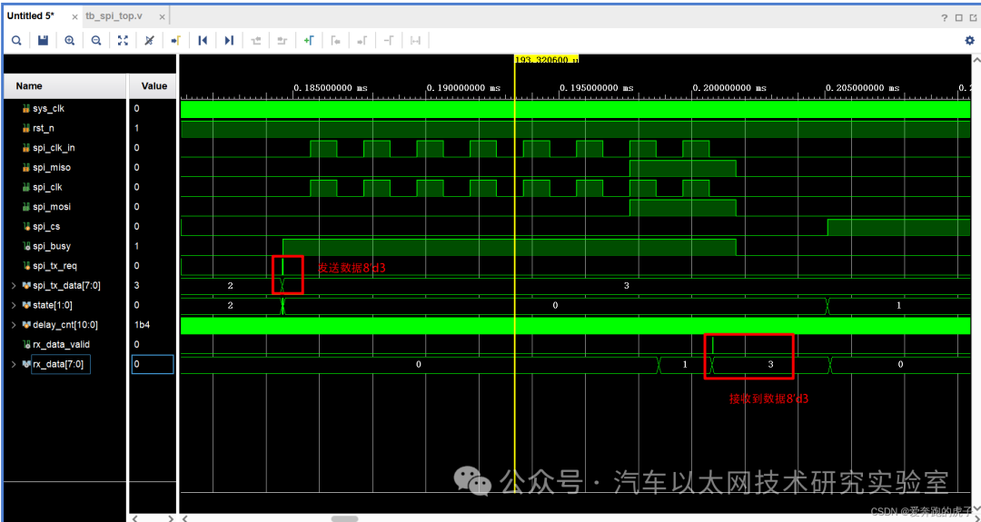
The top-level simulation sends incrementing numbers to the sender, which is then connected to the receiver, and the data reception is consistent.
8.3 On-Board Verification
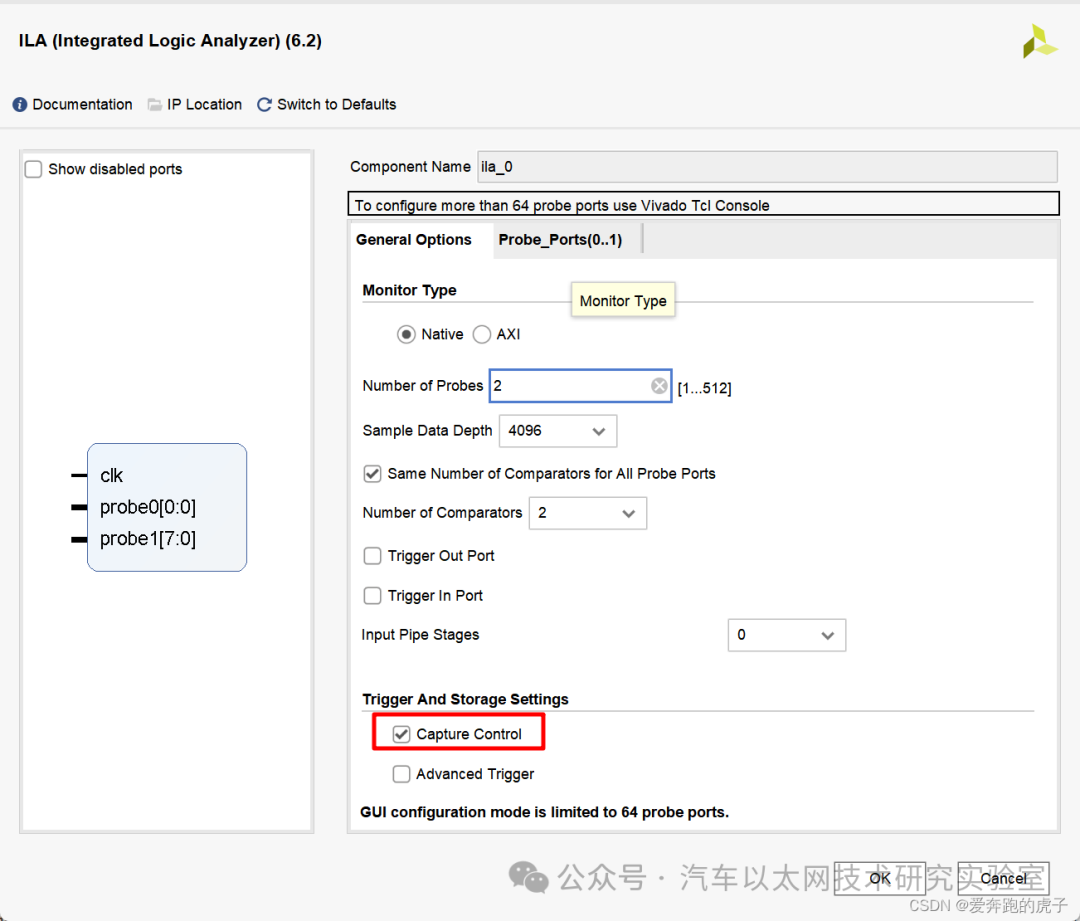
We instantiate an ILA to capture the rx_data and rx_data_valid signals in the spi_rx module and enable the capture mode. For specific capture mode principles and usage, please refer to the Vivado ILA Capture Control mode and Advanced Trigger functionality, as well as the TSM (Trigger State Machine) writing. The configuration diagram is as follows:
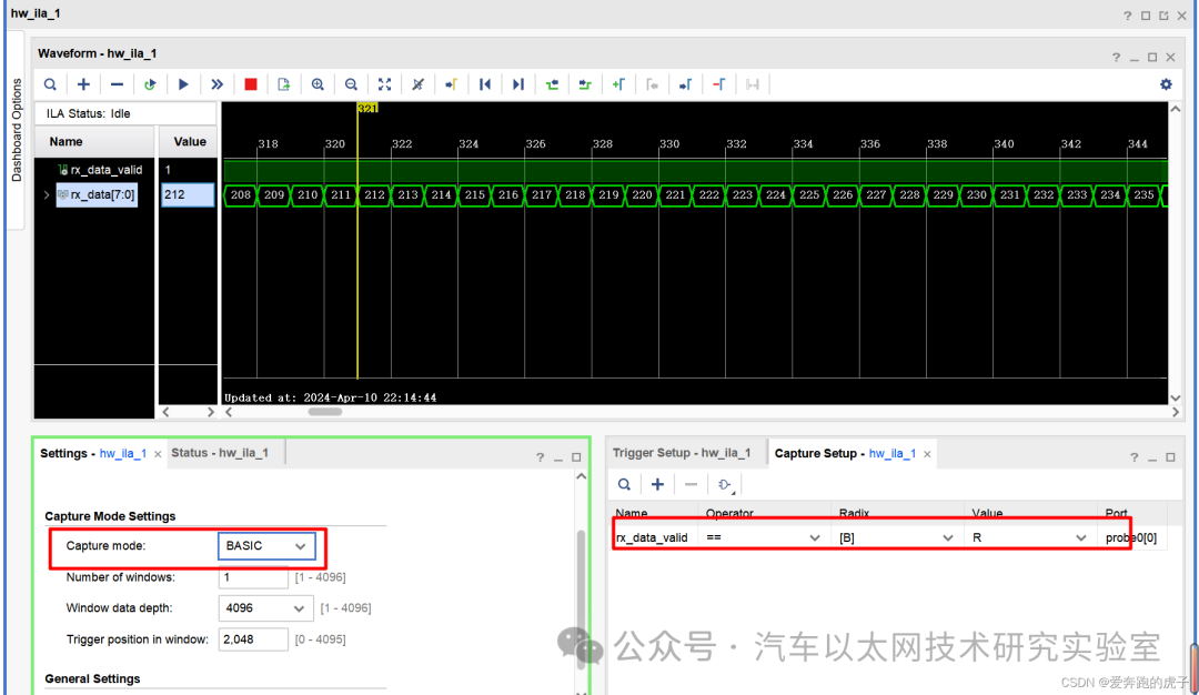
After downloading, we set the capture mode to BASIC and select the trigger condition as rx_data_valid. Observing the waveform, we find that the data is continuously incrementing, indicating that the SPI loopback was successful.



*Disclaimer: This article is original or forwarded by the author. If it inadvertently infringes on any party’s intellectual property rights, please inform us for deletion.
The above images and text are sourced from the internet. If there is any infringement, please contact us in a timely manner, and we will delete it within 24 hours.
The content of the article represents the author’s personal views, and the Automotive Ethernet Technology Research Laboratory reprints it only to convey a different perspective, which does not represent the Automotive Ethernet Technology Research Laboratory’s endorsement or support of this view. If there are any objections, please feel free to contact the Automotive Ethernet Technology Research Laboratory.
Original link:
https://blog.csdn.net/qq_43156031/article/details/137227371