FPGA stands for Field Programmable Gate Array, which is a type of programmable logic device. FPGA is a new high-performance programmable logic device developed based on CPLD, typically using SRAM technology, although some dedicated devices may use Flash technology or Anti-Fuse technology. FPGAs have a high integration level, with device densities ranging from tens of thousands to tens of millions of logic gates, capable of implementing very complex sequential and combinational logic functions, making them suitable for high-speed, high-density high-end digital logic circuit design. The basic components of an FPGA include programmable input/output units, basic programmable logic units, embedded RAM, rich routing resources, underlying embedded functional units, and embedded dedicated hard cores.
System designers can connect the internal logic blocks of the FPGA using editable connections, just like a circuit breadboard is placed inside a chip. The logic blocks and connections of a finished FPGA can be changed according to the designer, allowing the FPGA to perform the required logical functions.
Generally, FPGAs are slower than ASICs (Application-Specific Integrated Circuits), and the area required to implement the same function is larger compared to ASICs. However, they also have many advantages, such as quick product availability, the ability to modify designs to correct programming errors, and lower costs. Manufacturers may also offer cheaper FPGAs with limited editing capabilities. Due to their poor editing capabilities, the development of these designs is completed on standard FPGAs, and then the design is transferred to a chip similar to an ASIC. Another method is to use CPLD (Complex Programmable Logic Device). Generally, the complete FPGA design process includes major steps such as circuit design and input, functional simulation, synthesis optimization, post-synthesis simulation, layout and routing, post-layout simulation, board-level validation, and configuration debugging.

(1) Circuit Design and Input
Circuit design and input refer to the process of inputting the engineer’s circuit concept into EDA tools using certain standardized description methods. Common design input methods include Hardware Description Language (HDL) and schematic design input methods. Among HDLs, the most widely used are VHDL and Verilog HDL.
(2) Functional Simulation
After completing the circuit design, specialized simulation tools are used to perform functional simulation to verify whether the circuit functions meet design requirements. Functional simulation is sometimes referred to as pre-simulation. Common simulation tools include ModelSim, VCS, NC.Verilog, and NC.VHDL.
(3) Synthesis Optimization
Synthesis optimization refers to translating HDL language, schematics, etc., into a logical connection (netlist) composed of AND, OR, NOT gates, RAM, flip-flops, and other basic logic units, and optimizing the generated netlist based on targets and requirements (constraints), outputting netlist files in standard formats such as edf and edn for the FPGA vendor’s layout and routing tools to implement.
(4) Post-Synthesis Simulation
After synthesis, it is necessary to check whether the synthesis results match the original design by performing post-synthesis simulation. During simulation, the standard delay files generated during synthesis are reflected back into the synthesis simulation model to estimate the impact of gate delays.
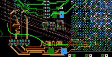
(5) Implementation and Layout Routing
The essence of the synthesis result is a logical netlist composed of AND, OR, NOT gates, flip-flops, RAM, and other basic logic units, which differs significantly from the actual configuration of the chip. At this time, software tools provided by FPGA vendors should be used to adapt the synthesized output logical netlist to the specific FPGA device based on the selected chip model; this process is called the implementation process. The main process in implementation is layout and routing. Layout (Place) refers to reasonably mapping the hardware primitives or underlying units in the logical netlist to the inherent hardware structure of the FPGA; routing (Route) refers to the process of correctly connecting various components based on the topological structure of the layout using various routing resources within the FPGA.
(6) Timing Simulation and Validation
Timing simulation, or post-layout simulation, is performed by reflecting the delay information from layout routing back into the design netlist. The primary purpose of post-layout simulation is to discover timing violations, which occur when timing constraints or inherent timing rules of the device (setup time, hold time) are not met.
(7) Board-Level Simulation and Validation
In some high-speed designs, it is also necessary to use third-party board-level validation tools for simulation and validation. These tools can analyze circuit characteristics such as signal integrity and electromagnetic interference (EMI) through simulations of the design’s IBIS, HSPICE, and other models.
(8) Device Download and Debugging
The final step in design development is online debugging or writing the generated configuration file into the chip for testing. Oscilloscopes and logic analyzers are the main testing tools for logical designs. If any simulation or validation step encounters issues, one needs to return to the corresponding step to modify or redesign based on the error location. Currently, there are two major FPGA device manufacturers, namely Altera from the USA and Xilinx. Altera’s FPGA products mainly include the Cyclone series and Stratix series, with the software development platform being Quartus II, while Xilinx’s FPGA products mainly include the Virtex series and Spartan series, with the software development platform being ISE.

Click the image for details on the winter camp.


Chengdian Youth Learning 100-Day Order Class is Hotly Launched!!! The think tank platform offers online and offline learning simultaneously. Series courses such as “Eight Lessons on FPGA Introduction”, “Ten Projects on FPGA Introduction”, and “Five Projects on FPGA Advanced” are available. The courses start from zero basics, with each lesson guiding students through a small experiment, learning FPGA courses step by step.
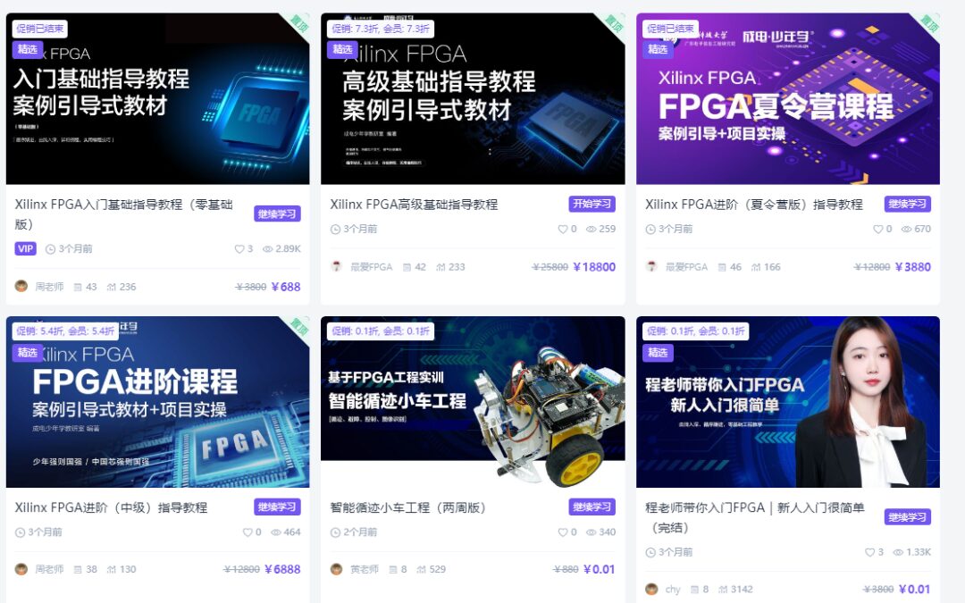

Since you’ve made it this far, why not follow us!! You can now apply for free to learn FPGA courses online, hurry up, time is limited! Course link: https://z.shaonianxue.cn. Students can follow our WeChat public account for continuous updates on FPGA industry consultation~~

For more details, consult:
Teacher Gao: 18935839030

END