
In recent years, the artificial intelligence industry has developed rapidly. McKinsey predicts that AI could contribute 1.2 percentage points to global GDP growth over the next decade, adding $13 trillion in value to global economic activity, comparable to the introduction of transformative technologies like the steam engine during the first Industrial Revolution.
From an industry chain perspective, artificial intelligence can be divided into three layers: the technological support layer, the basic application layer, and the product layer. Each layer is interlinked, with the basic and support layers providing the platform, resources, and algorithms for technological computation, while the development of the application layer relies on the basic layer and the application of technology.
Artificial Intelligence Industry Chain
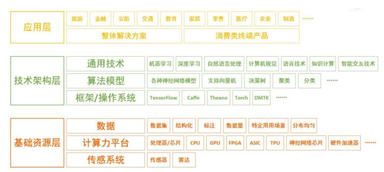
Source: KaiLian Capital Investment Research Department
The basic layer is divided into hardware and software. Hardware refers to chips with storage and computation capabilities, as well as sensors that acquire external data information; software refers to big data used for calculation. Here we focus on analyzing the hardware component of intelligent chips.
1. Intelligent Chips
From a technical architecture perspective, intelligent chips can be divided into general-purpose chips (CPU, GPU, FPGA), semi-custom chips based on FPGA, fully customized ASIC chips, and brain-like computing chips (IBMTureNorth). For the vast majority of intelligent needs, traditional computers based on general processors are costly, power-hungry, bulky, and slow, making them hard to accept. Therefore, computing chips represented by CPU, GPU, FPGA, ASIC, and brain-like chips are introduced into deep learning due to their high-performance computing capabilities.
AI Semiconductor Classification
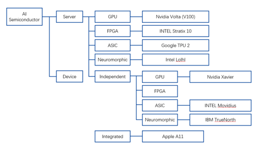
Source: Google, KaiLian Capital Investment Research Department
2017 AI Companies Public Chip Data
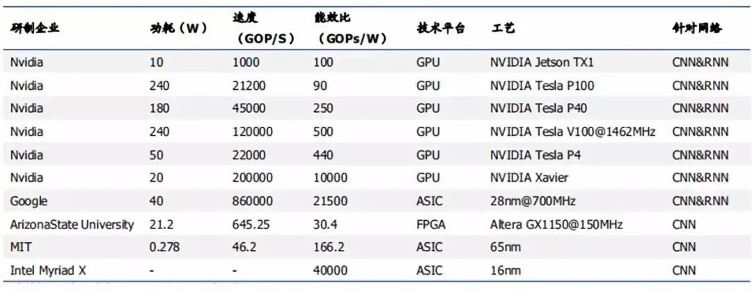
Source: Institute of Automation, Chinese Academy of Sciences, KaiLian Capital Investment Research Department
(1) GPU
Under large-scale data volumes, traditional CPU computing performance is limited. It follows the von Neumann architecture, which is based on: storing programs and executing them sequentially. With the advancement of Moore’s Law and the increasing demand for larger scale and faster processing speeds, the speed at which CPUs execute tasks is limited. GPUs have efficient parallelism in computation. GPU chips used for image processing were the first to be introduced into deep learning due to their massive data parallel computing capabilities. Most transistors in CPUs are mainly used to construct control circuits (such as branch prediction) and Cache, with only a small portion of transistors completing actual computation work. The design goals of GPUs and CPUs are different; their control circuits are relatively simple, and they have less demand for Cache, so most transistors can form various dedicated circuits and multiple pipelines, resulting in a breakthrough in GPU computation speed, with astonishing capabilities in processing floating-point operations.
Comparison of GPU and CPU Structures
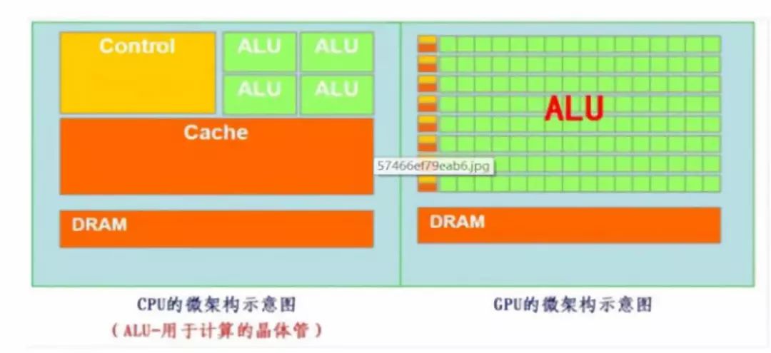
Source: Google, KaiLian Capital Investment Research Department
(2) FPGA
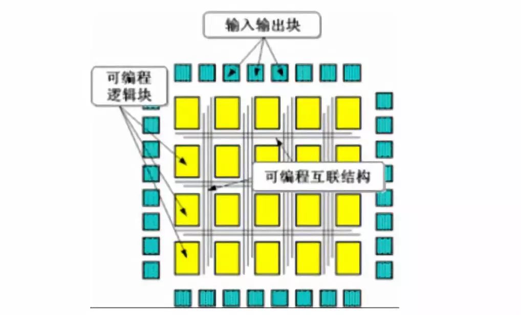
FPGA (Field Programmable Gate Array) is a chip that integrates a large number of basic gate circuits and memory, with the main feature of being programmable. It can define the connections between these gate circuits and memory by burning FPGA configuration files to achieve specific functions. Additionally, it can modify internal logic structures through instant programming, thereby achieving different logical functions. FPGAs have significant energy efficiency advantages, low latency, and high throughput characteristics. Unlike CPUs and GPUs that adopt the von Neumann architecture, FPGAs are mainly composed of programmable logic units, programmable internal connections, and input/output modules. The functions of each logic unit and the connections between logic units are determined after the program is written, so there is no need to fetch instructions or decode instructions during computation, and logic units do not need to communicate through shared memory. Therefore, although the main frequency of FPGAs is much lower than that of CPUs, the clock cycles required to complete the same computation are fewer than those of CPUs, resulting in significant energy efficiency advantages, with low latency and high throughput characteristics.
FPGA Structure Diagram
Source: Google, KaiLian Capital Investment Research Department
(3) ASIC
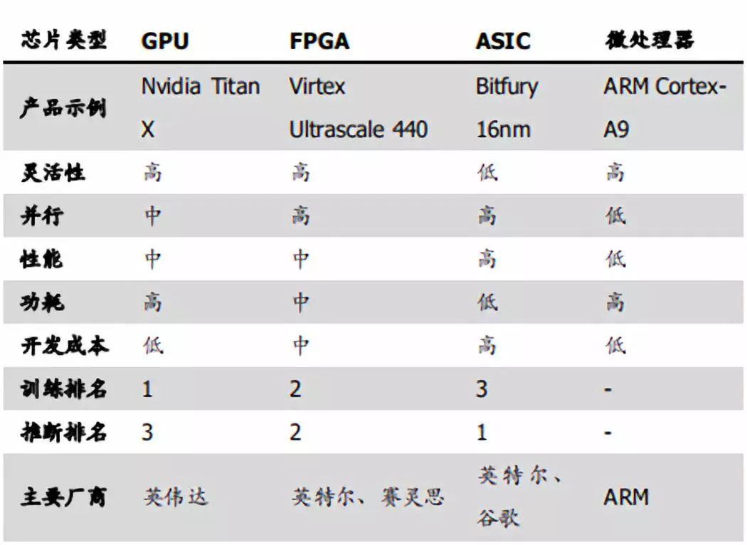
ASIC chips are custom chips designed to meet specific requirements. Aside from being non-expandable, they have advantages in terms of power consumption, reliability, and size, especially in high-performance, low-power mobile applications. Google’s TPU, Cambricon’s GPU, and Horizon’s BPU all belong to ASIC chips. Google’s TPU is 30-80 times faster than CPU and GPU solutions; compared to CPUs and GPUs, TPUs reduce control, thus decreasing chip area and power consumption. Its disadvantages include long development cycles and high investment costs, making it difficult for most companies to bear.
The Tensor Processing Unit (TPU) is a dedicated chip (ASIC) designed by Google for machine learning, specifically for Google’s deep learning framework TensorFlow. Compared to GPUs, TPUs use low precision (8-bit) calculations to reduce the number of transistors used in each operation. Reducing precision has little impact on the accuracy of deep learning, but it can significantly reduce power consumption and increase computation speed. Google first announced the TPU in 2016. The second-generation TPU was announced in 2017 and deployed on Google Cloud Platform, with a floating-point computing capability of up to 180 trillion operations per second.
Comparison of Main AI Chip Performances
Source: Academic Papers, KaiLian Capital Investment Research Department
2. Intelligent Chip Architecture
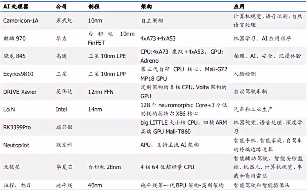
Architectural innovation is key to solving the rising costs. As the market demand for chip computing capabilities increases, chip manufacturing processes are also continuously improving, leading to rising chip manufacturing costs. The key to solving this issue is architectural innovation. Currently, the main architectures for AI chips include CPU+GPU, CPU+FPGA, CPU+ASIC, etc.
Mainstream AI Processors’ Manufacturing Processes and Architectures
Source: Electronic Enthusiasts, KaiLian Capital Investment Research Department
3. Applications of Intelligent Chips
Deep learning mainly consists of two stages: training and inference. In the data training (training) phase, a large amount of labeled or unlabeled data is input into the deep neural network for training. As the number of layers in the deep neural network model increases, the corresponding weight parameters grow exponentially, leading to a higher demand for hardware computing power. The design goal at this stage is high concurrency and high throughput.
Inference (inference) is divided into two categories—cloud-side inference and edge-side inference. Cloud-side inference not only requires hardware to have high-performance computing but also emphasizes the ability to handle multiple instruction data. For example, the Bing search engine must recognize and infer thousands of image search requests simultaneously to provide search results; edge-side inference emphasizes finding a balance between high-performance computing and low power consumption, with design goals of low latency and low power consumption.
Therefore, based on current market demand, artificial intelligence chips can be categorized into three types:
1) Chips for training: These mainly target the training segment of major AI companies and laboratories. The widely accepted model in the industry is the