The CAN bus, as a core communication protocol in the automotive and industrial fields, achieves high-reliability multi-node communication through differential signaling and non-destructive arbitration. Its physical layer uses CAN_H and CAN_L to transmit differential signals over a two-wire system, distinguishing between dominant (logic 0) and recessive (logic 1) states through voltage differences. Coupled with 120Ω termination resistors at both ends of the bus to match impedance, this reduces signal reflections. When multiple nodes send data simultaneously, CAN employs a bit-wise arbitration mechanism based on identifiers, allowing the message with the smallest ID value to have the highest priority for transmission, ensuring communication efficiency.
NXP’s TJA1043, as a third-generation high-speed CAN transceiver, is a key interface device between the physical layer and the data link layer. It fully complies with the ISO 11898 standard, supporting both traditional CAN and CAN FD protocols, with data rates up to 5Mbit/s in fast phase. This chip implements signal conversion between the microcontroller and the bus: converting the TXD logic signal into a differential signal sent to the bus, while demodulating the differential signal from the bus back into RXD logic levels for the controller.

Operating Modes of TJA1043
The TJA1043 provides five operating modes, utilizing pins STB_N (standby control, active low) and EN (enable) for mode selection. The different modes are designed to balance functionality and power consumption between normal communication and low-power sleep, supporting both remote and local wake-up. The transition relationships between modes can be referenced in its state diagram. Below, the functions, switching conditions, and application scenarios of each mode are introduced:
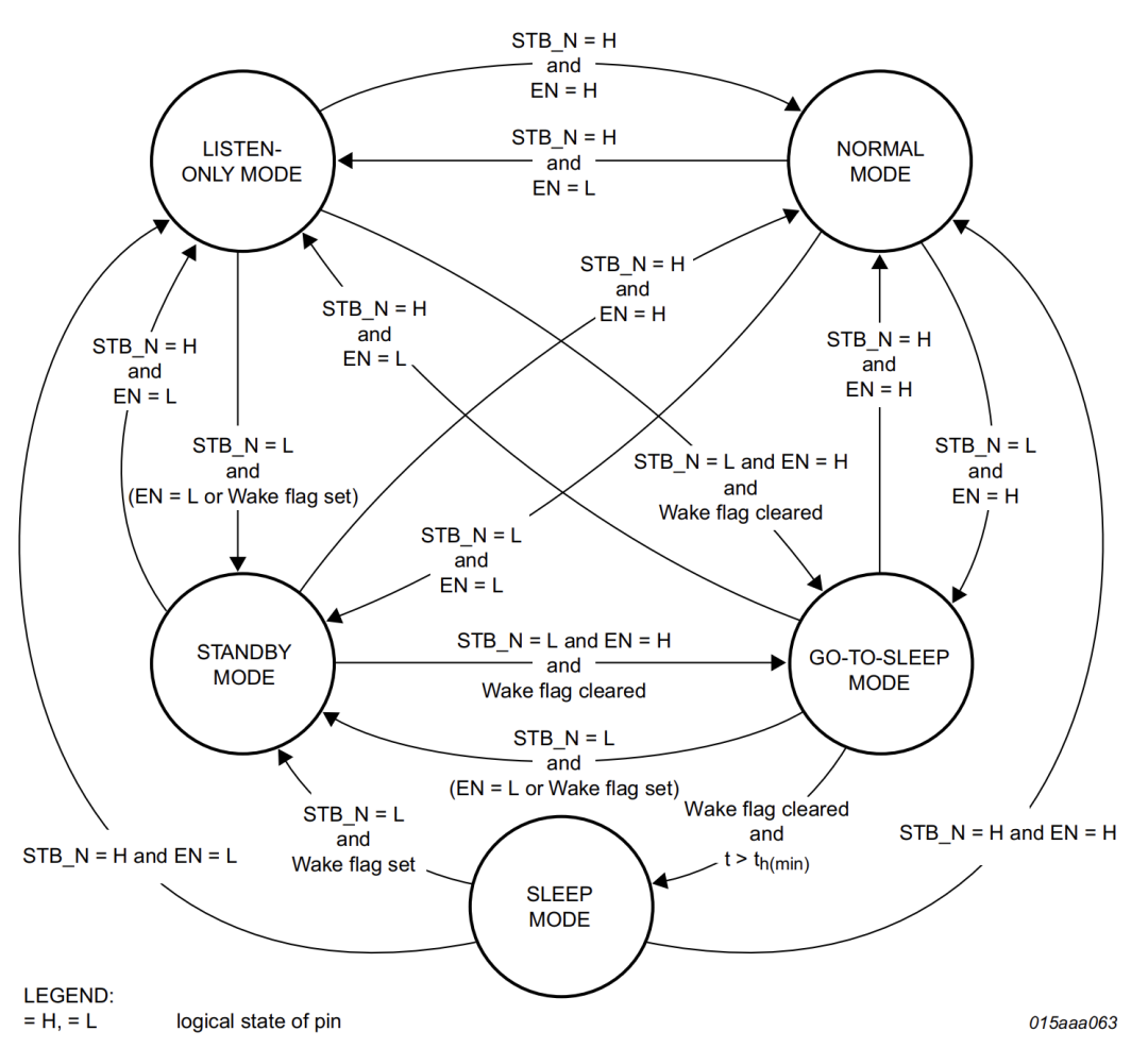
Normal Mode: The transceiver is in full functional state, capable of sending and receiving bus data through CANH/CANL. The differential receiver of the transceiver converts the bus analog signal into a digital signal output to the RXD pin; the transmitter drives the bus based on the input from the TXD pin. The rise/fall edges of the output waveform are internally optimized to reduce electromagnetic radiation (EME). In normal mode, the two bus wires are biased at approximately 0.5*Vcc (typically around 2.5V) as a recessive level to ensure stability when the bus is idle. At this time, the INH pin is active high, typically used to power the node’s voltage regulator.Application Scenario: Used when nodes are communicating normally, capable of sending and receiving CAN messages.
Listen-Only Mode: Also known as monitoring mode. In this mode, the transmitter of the transceiver is disabled, and only the receiver operates, effectively acting as a “listening” node. The bus signals on CANH and CANL are still converted to digital output on RXD, but the transceiver itself does not send any data to the bus. Similar to normal mode, the bus is still internally biased at 0.5*Vcc, and INH remains active.Application Scenario: Used for node diagnostics and fault isolation. When a node may malfunction and disrupt the bus, it can be placed in listen-only mode to only monitor the bus without interfering with communication. For example, a node that enters the **Bus-Off** state can resume monitoring bus traffic in listen-only mode.
Standby Mode: The first level low-power mode of the TJA1043, reducing node current consumption. In standby mode, the transceiver cannot send or receive normal data frames; only a low-power receiver is operational to monitor bus activity. The bus pins are pulled down to near ground potential (approximately 0V in recessive state) (Note: other normal nodes maintain the bus recessive level, so this node does not interfere with the bus).The INH pin remains active high in standby mode, meaning the external regulator it controls remains on, allowing the main microcontroller to continue operating. When a wake-up event occurs on the bus or a local wake-up is triggered, the transceiver reflects the active wake-up request through the RXD and ERR_N pins (requiring VIO voltage to be present).Application Scenario: Used when a node needs to temporarily refrain from participating in bus communication but maintain monitoring of bus activity and respond quickly. For example, after parking, the ECU enters standby energy-saving mode but can immediately wake up and continue working upon receiving a CAN message or local signal.
Go-to-Sleep Mode: This is a control mode transitioning from standby to sleep. The transceiver behaves similarly to standby mode but begins executing the sleep command simultaneously. Once the host sets STB_N from low to high and EN to high, it indicates a request to enter sleep. The TJA1043 will remain in the “Go-to-Sleep” mode for a hold time of t<sub>h(min)</sub> before actually switching to sleep mode. If a wake-up flag is detected before the hold timing ends (a wake-up event on the bus or WAKE pin) or the state of the STB_N/EN pins changes, the transceiver will abort entering sleep and revert to standby/normal mode.Application Scenario: Used for orderly system shutdown. A brief time is allowed before switching to sleep to handle pre-sleep tasks or prevent accidental entry into sleep mode. For example, after sending a sleep command, wait briefly to confirm no bus activity before entering sleep.
Sleep Mode: The second level (deep) low-power mode of the TJA1043. Entering sleep must go through the aforementioned “Go-to-Sleep” process or automatically enter during power loss. In sleep mode, the transceiver behaves similarly to standby mode: normal transceiving functions are disabled, retaining only low-power monitoring. The difference is that the INH pin is set to high impedance (floating), thus turning off the external regulator it controls, completely powering down the node (including the microcontroller) to achieve the lowest current consumption at the “node power-off” level. The part of the TJA1043 powered by the VBAT battery remains operational, listening for wake-up events on the CAN bus and WAKE pin. Once a remote wake-up mode on the bus is detected (see below) or a valid transition on the local WAKE pin occurs, or the host raises the STB_N/EN pins, the TJA1043 will wake the node from sleep. The process is as follows: the INH pin outputs high to turn on the regulator, the RXD outputs a low pulse to notify the microcontroller of the wake-up source, and then switches to standby mode waiting for further actions from the host.Application Scenario: Used when CAN communication is not needed for an extended period, allowing the ECU to enter sleep mode (e.g., after the vehicle is turned off), reducing node power consumption to microamp levels while maintaining responsiveness to wake-up events.
Wake-Up Mechanism: The TJA1043 supports both local wake-up (via the WAKE pin) and remote wake-up (via the CAN bus). The WAKE pin can be connected to events such as door switches; when a transition from low to high or high to low is detected and stable for a certain time, a local wake-up request is generated. Remote wake-up follows the wake-up mode defined in ISO11898-2:2016: a specific pattern of level changes on the bus—at least t<sub>wake(dom)</sub> time of dominant level, then t<sub>wake(rec)</sub> time recessive, followed by another dominant, and the entire sequence completed within t<sub>to(wake)</sub> time window—can be recognized as a remote wake-up. This mode avoids false wake-ups from brief disturbances. When the TJA1043 detects the above wake-up sequence while in standby or sleep, it sets the wake-up flag and outputs a low pulse on the RXD pin to notify the microcontroller. After waking up, the transceiver will enter standby mode, waiting for the host to switch it to normal mode.

Electrical Characteristics of CAN Transceivers
Driving and Level Definitions: The TJA1043 complies with the ISO 11898-2 physical layer standard, corresponding to the differential driver and receiver characteristics of high-speed CAN bus. The CAN bus uses two differential lines: CANH (high level line) and CANL (low level line). The transceiver controls the voltages on these two lines to achieve dominant and recessive logic levels: when dominant (representing binary “0”), the driver makes the CANH voltage higher than CANL by about 2V; when recessive (representing “1”), the driver does not actively drive, and the voltages on both lines tend to be the same. Typically, at Vcc=5V, in the dominant state, CANH≈3.5V, CANL≈1.5V, and the differential voltage V<sub>dif</sub> is about 2V; in the recessive state, both lines are biased at about 2.5V, i.e., CANH≈CANL≈0.5*Vcc, with a differential voltage of approximately 0V. The bus recessive level is provided by a stable DC bias from the transceiver’s internal bias network, which can be further improved in stability through the TJA1043’s SPLIT pin (see subsequent EMC characteristics). The receiver uses differential comparison, determining dominant when the CANH–CANL differential voltage exceeds the threshold (about 0.7V); otherwise, it is recessive. The TJA1043 receiver includes hysteresis design (typically about 0.12V) to enhance noise immunity. For example, in normal mode, the differential threshold range is about 0.5–0.9V, ensuring that a differential voltage >0.9V is reliably recognized as dominant, and <0.5V as recessive. This design allows for a certain amplitude of signal disturbance without causing misjudgment.
Common Mode Range and Immunity: CAN transceivers need to adapt to different node ground potential differences. The TJA1043’s receiver can reliably detect differential signals within a common mode voltage range of -30V to +30V. This means that even if two nodes have ground differences of several tens of volts (such as during ground loop voltage), communication can still occur as long as the differential voltage reaches the threshold. This wide common mode range increases tolerance to ground offsets in automotive applications. The input resistance of the transceiver’s bus pins to ground is typically about 30 kΩ (in differential mode), with symmetry error within ±3%. High input impedance ensures that even when multiple nodes are connected, the bus is not significantly loaded (the typical network has two terminal resistors of 60Ω×2 in parallel = 30Ω, far less than the node leakage impedance). Additionally, the TJA1043’s bus pins have low equivalent capacitance (about 20pF common mode, about 10pF differential), reducing the impact on high-speed signals.
Electromagnetic Compatibility Performance: The TJA1043 has enhanced EMC characteristics for automotive applications, including reduced radiated emissions and improved immunity to electromagnetic interference. Its driver output uses controlled rise/fall times to limit transient current change rates, reducing cable radiation. Actual tests show that compared to previous generation devices, this series can meet strict automotive EMI/EMC requirements without the need for common mode chokes. The transceiver provides a SPLIT pin for common mode stabilization: in normal and listen modes, the SPLIT outputs a DC voltage of about 0.5*Vcc, which can be connected to the midpoint of the bus (the midpoint of the terminal resistors) to stabilize the bus recessive common mode level. Typically, the SPLIT pin is connected to the midpoint of two terminal resistors of 60Ω, with a 4.7nF capacitor to ground to filter out common mode noise (this is the “Split Termination” topology), effectively suppressing disturbances to the common mode caused by bus DC leakage due to node power-off, reducing electromagnetic emissions. In standby/sleep modes, to avoid power consumption, the SPLIT pin becomes high impedance and no longer drives voltage.
Transient Protection and ESD: The bus transceiver part of the TJA1043 can withstand harsh electrical conditions in automotive environments. According to the datasheet, the absolute maximum voltage for the VBAT power pin can reach +58V (such as during load transients), and CANH/CANL can withstand ±20V differential voltage. The bus pins and VBAT can withstand transient pulses of up to ±100V (in compliance with ISO16750-2 standard pulses 1, 2a, 3a, etc.). The device’s ESD immunity is also very high: the CANH/CANL pins to ground can withstand electrostatic discharge up to ±8 kV (contact discharge) in accordance with IEC61000-4-2 standards. This means that generally, no additional ESD protection components are needed to meet mainstream OEM requirements. Nevertheless, in actual designs, transient suppression diodes (TVS) and common mode inductors can be added to the transceiver’s bus pins as needed to further enhance surge and EMI performance. The TJA1043 has a bus disturbance-free characteristic during power-off: when VBAT is powered off, the transceiver automatically disconnects from the bus and enters a high-impedance state (not “pulling down” the bus when unpowered). At the same time, its TXD, STB_N, and other input pins have internal bias to prevent uncertain states when floating. These designs ensure that the transceiver’s behavior is predictable under various power supply conditions and does not inadvertently interfere with the network.
CAN Protocol Frame Structure and Working Principles
Frame Types and Structures: The information transmitted over the CAN bus is referred to as a message. When the bus is idle, any node can initiate a new message. CAN defines five types of frames: data frames, remote frames, error frames, overload frames, and frame intervals. Among them, the data frame is used to send actual data carried by the node, while the remote frame is used to request a data frame for a certain ID, both of which have standard and extended formats; error frames and overload frames are automatically sent by the protocol for error signaling and delay requests; the frame interval is used for spatial isolation between frames. This article focuses on the data frame and protocol mechanisms. A standard data frame consists of seven fields, as shown in the figure:
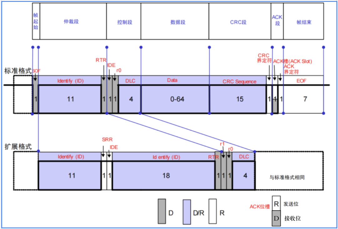
Illustration of standard frame and extended frame structure. The purple shaded areas indicate the bit lengths of each segment of the frame, the red annotations are control bits (RTR/IDE, etc.), and the black numbers indicate bit lengths. The upper part shows the standard frame format with an 11-bit ID, while the lower part shows the extended frame format with a 29-bit ID.
Frame Start (SOF): Composed of 1 dominant bit (0), marking the start of the data frame. When the bus is idle, it is at a recessive level (1); once a node sends the SOF dominant bit, other nodes immediately synchronize to this bit and begin receiving the frame.
Arbitration Field: Used for arbitration of bus priority, including identifier ID and additional control bits. The standard format arbitration field contains an 11-bit identifier; the extended format arbitration field contains a 29-bit identifier (composed of an 11-bit base ID and an 18-bit extended ID). Additionally, there are RTR/SRR and IDE bits: the RTR (remote request) bit is used to distinguish between data frames and remote frames, being dominant 0 in data frames and recessive 1 in remote frames; the IDE (identifier extension) bit indicates whether it is an extended frame, with standard frames having IDE as dominant 0 and extended frames as recessive 1. In extended frames, there is also an SRR (substitute remote request) bit, occupying the position of RTR in standard frames and fixed as recessive, ensuring that during arbitration, the 11-bit ID standard frame can take priority over the same ID starting extended frame (because the standard frame sends dominant 0 at this bit, while the extended frame SRR is 1, which is overridden by the dominant).
Control Field: 6 bits in length, containing data length code DLC and reserved bits. DLC is 4 bits, indicating the number of bytes in the data segment (0 to 8 bytes, up to 64 bytes for CAN-FD, but a maximum of 8 in classic CAN). The standard frame control field consists of IDE, r0, and DLC, while the extended frame consists of IDE, r1, r0, and DLC.
Data Field: The actual data content transmitted, which can be 0 to 8 bytes (standard CAN). When DLC is less than 8, the remaining bytes are not sent. The remote frame does not have a data field, only the aforementioned DLC to indicate the requested data length.
CRC Field: The cyclic redundancy check field used to detect frame transmission errors. It includes a 15-bit CRC sequence and a 1-bit fixed recessive CRC delimiter. The sending node calculates the 15-bit CRC value based on all bits from the frame start to the data field and appends it to this field for transmission. The receiving node also calculates the CRC for the received data and compares it to verify data integrity. The CRC delimiter is a 1-bit recessive used to mark the end of the CRC segment.
Acknowledgment Field (ACK): Contains the acknowledgment bit and acknowledgment delimiter, each 1 bit. The sending node sends recessive bits during these two slots. If at least one receiving node correctly receives the frame, it will pull the bus to dominant 0 during the ACK acknowledgment bit period to indicate “received,” which serves as confirmation to the sender. The subsequent ACK delimiter is maintained as recessive by the sender to restore the bus to recessive level. If the sender detects recessive in the ACK slot (indicating no acknowledgment), it can determine that this frame was not received and will initiate a retransmission or error handling.
Frame End (EOF): 7 recessive bits, marking the end of a frame. The frame interval then contains at least 3 recessive bits as the inter-frame space, allowing the bus to return to idle and ensuring separation between frames. In cases of errors on the bus, the frame interval has corresponding extensions (e.g., an error-active node must wait for 8 recessive bits of “suspended transmission” after the inter-frame space). In normal communication, as long as the bus detects 11 consecutive recessive bits (EOF + IFG), it can be deemed idle, and any node can initiate the next SOF.
Bit Stuffing: In data frames and remote frames, from SOF to the end of the CRC sequence, CAN uses bit stuffing encoding to ensure signal synchronization and avoid false flag sequences. The rule is: whenever the sender encounters 5 consecutive identical logic bits (whether 5 zeros or 5 ones) in the frame bit stream, it automatically inserts a bit of the opposite polarity immediately after. For example, if the data segment has five consecutive dominant 0s, the sender will insert a recessive 1, then continue sending the original data bits. The receiving node will automatically remove these stuffed bits upon detection of this pattern, restoring the original data content. The purpose of bit stuffing is twofold: first, to prevent long strings of identical bits from being misinterpreted as error frames or frame ends (for example, a long string of dominant bits ‘0’ could be mistaken for an error flag or EOF), thereby improving transmission reliability by limiting the length of consecutive identical bits; second, to provide sufficient level transitions for synchronization. CAN is a clockless encoding, and bus nodes rely on level transitions in the bit stream to maintain bit synchronization. The bit stuffing mechanism ensures that there is a level transition at least once every five bits (either the inserted bit itself or the original data that should have transitioned), providing synchronization opportunities for all nodes. It is important to note that bit stuffing does not apply to fixed format fields such as the CRC delimiter, ACK field, and EOF field, which do not participate in stuffing; additionally, error frames and overload frames also do not have a bit stuffing mechanism. The receiver also checks the bit stuffing rules: if it detects 6 consecutive identical bits in areas requiring stuffing without an inserted bit, it will determine a stuffing error, triggering an error flag frame.
Arbitration Mechanism: The CAN bus uses “wired-AND” logic, meaning the physical bus level is the logical AND result of the outputs from all nodes—dominant is equivalent to logic 0, recessive is equivalent to logic 1, and 0 ANDed with any 1 is 0. Therefore, when multiple nodes transmit simultaneously, dominant levels take priority: as long as one node outputs dominant (0), the bus will present a dominant level, overriding other nodes sending recessive. Utilizing this principle, CAN achieves bit-level arbitration: in the arbitration field, all nodes that start sending will synchronize to send their respective ID bits while listening to the actual bus level. When a node sends a recessive “1” but detects the bus as dominant “0”, it indicates that a higher priority (smaller ID) message exists, and this node will automatically cease transmission (switching to receive mode), while the priority node continues to send. The entire arbitration process is completed without losing bit timing or incurring losses, meaning that the backing-off node exits while the bus has not yet encountered an error, allowing the priority frame to continue sending directly. Ultimately, the node with the smallest ID value (i.e., the highest priority binary code) wins and gains control of the bus. For example, if two nodes send standard frames with IDs of 0x123 (binary 0100100011) and 0x11E (binary 0010001110) simultaneously, they start with the same initial 0, and arbitration occurs bit by bit. When comparing a certain bit, if one node outputs 1 and the other outputs 0, the bus becomes dominant = 0, and the node outputting 1 detects its loss and immediately stops sending. This ensures that the lowest ID wins, reflecting the mechanism by which CAN uses ID to determine message priority. It is particularly noteworthy that when both standard and extended frames exist, if two nodes have the same 11-bit ID, but one is a standard frame (IDE=0) and the other is an extended frame (IDE=1), then at the 12th bit (the IDE bit), the standard frame sends dominant 0 while the extended frame sends recessive 1, resulting in the bus being dominant 0, causing the extended frame node to detect arbitration failure and exit. Therefore, the priority of standard frames is always higher than that of extended frames (as long as the two have the same 11-bit base ID). Similarly, when a remote frame (RTR=1) and a data frame (RTR=0) contend for arbitration with the same ID, the data frame will win by sending dominant 0 at the RTR bit, ensuring that the request frame does not suppress actual data transmission. Through the arbitration mechanism, the CAN network ensures that only one node successfully transmits when multiple nodes send simultaneously, while the other nodes automatically back off without needing to retransmit the bits sent before arbitration, achieving high efficiency.
CRC Check and Error Handling: The receiving node calculates its own CRC after receiving a complete frame and compares it with the CRC field check value. If they do not match (or frame format, stuffing, etc. checks fail), the receiving node will determine that a transmission error has occurred and immediately send an error flag frame to notify the bus. The error flag sent by the active error node consists of 6 dominant bits (violating the bit stuffing rule, causing other nodes to synchronize incorrectly); the passive error node sends 6 recessive bits as the error flag. The error flag will immediately corrupt the original frame’s CRC delimiter or EOF, causing all nodes to detect the error and discard the frame. The bus then enters the error frame end and frame interval process, and after certain conditions are met, the erroneous frame will be automatically retransmitted by the sending node. The CAN error management mechanism ensures reliable data transmission: any error point will be detected and quickly notified to the network, with each node maintaining an error counter to determine its own status (active error/passive/error bus off). These mechanisms exceed the scope of this article, but it is important to understand that CRC and error frames together provide robust error detection and correction capabilities, giving CAN high transmission reliability.

Connection Method of TJA1043 in Typical Application Circuits
The TJA1043, as a CAN transceiver, is typically integrated into the ECU node, connecting one side to the microcontroller (CAN controller) and the other side to the CAN bus. Below, a typical circuit is used to illustrate the connections of each pin and the configuration of commonly used external components.
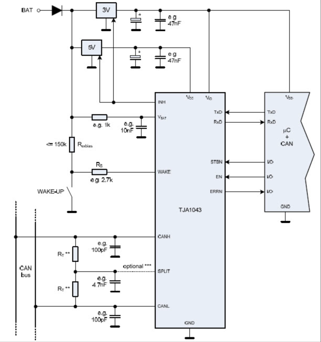
The typical application circuit of TJA1043 paired with a 3V microcontroller. The figure shows the typical connections of each pin of TJA1043 with the microcontroller, power supply, battery, and CAN bus, as well as recommended external components (such as terminal resistors, common mode inductors, filter capacitors, voltage regulators, etc.).
Connection with Microcontroller
As shown in the figure, the microcontroller’s CAN controller typically provides transmit data (TXD) and receive data (RXD) pins. The TXD pin connects to the TXD input of the TJA1043, controlling the transceiver to drive the bus dominant/recessive; the RXD pin receives the bits listened to on the bus from the RXD output of the TJA1043. To accommodate different MCU levels, the TJA1043 provides an independent VIO pin, which should be connected to the digital power supply voltage of the microcontroller (e.g., 3.3V or 5V). This way, the high and low thresholds of TXD, RXD, and mode control pins STB_N, EN, ERR_N, etc., are adjusted based on the VIO voltage, achieving direct interfacing with the main controller.
The STB_N and EN pins are controlled by the microcontroller’s GPIO to switch the TJA1043 operating modes (as detailed above), for example, pulling STB_N high/low to exit or enter standby. The ERR_N pin is the fault output of the transceiver, with an open-drain or weak pull-up structure (active low). In normal mode, ERR_N can indicate remote wake-up events (Wake-up Source) or bus fault statuses; in listen mode, ERR_N can output local fault flags for the main controller to poll. Typically, ERR_N is connected to the MCU’s interrupt pin or IO for timely response to error/wake notifications.
The WAKE pin is used for local wake-up input, which can be connected to events such as ignition switches, door lock signals, etc. When WAKE detects a valid transition and remains stable for longer than the internal filter time of TJA1043, it will set the wake-up flag internally. In typical circuits, the WAKE pin often uses pull-down or pull-up resistors (R<sub>bias</sub>) for biasing, and is triggered by a switch or signal to pull it low/high. For example, in the figure, a ~150kΩ pull-up to the battery, a series 1k current-limiting resistor, and a 10nF capacitor for filtering are used, triggered by an open-drain switch, which both debounces and limits the leakage current (approximately VBAT/150kΩ). When not using the WAKE function, it is recommended to connect WAKE directly to VBAT or ground to reduce the impact of floating noise on EMI.
The power pins of TJA1043 include the main power supply VCC and battery power VBAT. VCC is generally connected to a +5V regulated output to power the transceiver’s transceiving circuit. VBAT connects to the vehicle battery voltage (typically +12V), powering the transceiver’s wake detection and other circuits, allowing it to monitor the bus even when VCC is powered off (in sleep). The figure shows two regulators providing 5V (for transceiver VCC) and 3V (for MCU), with their enable pins controlled by the INH pin of TJA1043.
The INH pin is the wake maintenance output of the transceiver: in normal mode, it is high to turn on external main power; in sleep mode, INH becomes high impedance, thus turning off the external regulator to achieve power-off sleep. As shown in the figure, the outputs of the two regulators are controlled by INH, ensuring that when the transceiver is in sleep mode, both the MCU and its own VCC power supply are turned off. The specific implementation of the regulators can be chosen based on design; some use INH to drive transistors or relays to cut off power, while others drive enable pins. Additionally, to ensure the transceiver is safe during battery transients or power loss, it is recommended to place a 1kΩ resistor in series with the VBAT pin to limit surge currents and add a 10nF capacitor to ground to filter transients. In practice, these values can be adjusted according to OEM specifications.
Connection and Termination Configuration with CAN Bus
The CANH and CANL pins of TJA1043 are connected to the vehicle CAN bus via shielded or unshielded twisted pairs. On the circuit board, the wiring of CANH/CANL requires equal length, close proximity, and differential routing to minimize noise (typically, the spacing between the two wires should be as close as possible, and the total length should not exceed 10cm to avoid common mode loops).Bus termination resistors are crucial for the proper functioning of the CAN network: typically, each bus end node connects a resistor of about 120Ω across CANH and CANL, forming a total of about 60Ω bus matching impedance to prevent signal reflections. If the TJA1043 node is configured as a bus end, a total of 60Ω + 60Ω equivalent termination should be connected between its CANH and CANL. There are two common approaches: one is to directly solder a 120Ω resistor across CANH–CANL; the other is to use Split termination, which involves two approximately 60Ω resistors connected from CANH and CANL to a branch point, which is then connected to ground through a capacitor, while also connecting to the SPLIT pin of the transceiver. The second scheme utilizes the SPLIT output of 0.5Vcc to stabilize the common mode of the bus recessive state and improve EMC performance (as mentioned earlier), thus being recommended. The figure indicates “R<sub>T</sub>≈60Ω, optional SPLIT” for this configuration. The example in the figure shows each bus line with a 30Ω termination resistor (two in parallel equal 60Ω) connected to SPLIT, which can be seen as a simplified representation; two 60Ω resistors can achieve the same effect. If this node is not a bus end (e.g., if there are independent centralized terminations on the bus), then a 120Ω hard termination should not be connected to avoid excessively lowering the bus impedance. However, sometimes, according to OEM requirements, a “weak termination” may be added to non-end nodes to improve the steady state when the bus is idle, such as using a resistor of about 1.3kΩ across CANH–CANL. This weak termination resistance is much larger than 60Ω, does not significantly affect the signal, but can provide some load when all actual terminations are powered off, depending on the specifications.
Bus filtering and protection: Passive components are often added to the CANH and CANL lines to enhance interference immunity. A common mode choke is often placed between the transceiver bus pins and the external connector; it presents high impedance to common mode noise and low impedance to differential signals. Thus, when common mode RF interference occurs on the bus or common mode noise due to imperfect driving, the choke will suppress its propagation, thereby reducing electromagnetic emissions and improving noise immunity. Due to the enhanced symmetry of the output stage and the application of SPLIT regulation, the official statement indicates that in most cases, it is possible to pass automotive EMC tests without using a choke; however, in high-demand situations, a small leakage inductance twisted pair common mode inductor (<500nH leakage inductance) can be selected for further filtering. It is recommended to place the choke as close to the transceiver pins as possible, and the routing of CANH/L should go through the inductor and ESD devices before reaching the connector to minimize parasitic oscillation. Additionally, matching capacitors are often connected in parallel to ground on each of CANH and CANL (for example, each line connected to ground with 100pF in the figure). This forms a bypass for common mode high-frequency noise, aiding in passing EMS immunity (static electricity, etc.) tests. The capacitor values should be chosen carefully: too large a value can affect the rise and fall edges of the bus signal and overall loop stability. Typically, the ground capacitance for each line should not exceed 470pF; at rates of 125kbps and below, it can be relaxed to several hundred pF, but at 500kbps and above, it is best to keep it below 100pF. Therefore, 100pF is a commonly used value that can filter RF interference without significantly affecting the signal. If a common mode inductor is already used, this ground capacitor should be placed after the inductor, close to the connector, to form L-C filtering for common mode noise. Finally, to guard against ESD and transient spikes, transient voltage suppression diodes (TVS) are often connected in parallel to ground or power on the CANH and CANL lines. For example, NXP’s PESD1CAN series ESD protection diodes have low capacitance and fast response, capable of limiting IEC 8kV ESD to safe levels. If using TVS, they are typically placed near the ECU’s external connector. The TJA1043 itself has high ESD tolerance (8kV contact discharge), so in some OEM designs, additional ESD components can be omitted; however, for higher protection needs or as a precaution, TVS diodes remain a simple and effective protective measure.
Decoupling and Layout: Sufficient decoupling capacitors should be placed close to the power pins. Typically, a combination of 47 µF electrolytic or tantalum capacitors and 100 nF surface mount ceramic capacitors is placed from the VBAT pin to ground, while at least 100 nF surface mount capacitors are placed for VCC and VIO, arranged close to the pins. As shown in the figure, both the 3V and 5V regulated outputs are equipped with 47 nF capacitors for filtering (larger values, such as 10 µF capacitors, can be used in practice, along with 0.1 µF high-speed capacitors in parallel). The INH control pin is recommended to have pull-up or pull-down resistors (in the kΩ range) added as shown in the figure to ensure that the voltage regulator defaults to the off state when the transceiver is not operational. In terms of PCB routing, the lengths of the CANH and CANL traces should be equal and adjacent to maintain impedance matching and reduce electromagnetic loop area. Digital signal lines (TXD, RXD, etc.) should avoid running close to analog bus traces to minimize crosstalk. A good ground plane and short decoupling loops also contribute to the system’s EMC performance.
TJA1043’s Fault Diagnosis and Protection Mechanisms
As an advanced transceiver, the TJA1043 integrates a rich set of fault detection and protection features, including bus short-circuit monitoring, transmission fault detection, over-temperature protection, and undervoltage power-off detection. When an abnormal condition is detected, the transceiver will take measures such as shutting down output drive and reporting flags through the ERR_N pin to prevent fault escalation and assist the host in diagnosis. The following sections introduce the principles of the main mechanisms:
Bus Short-Circuit Fault Detection
The TJA1043 can detect short-circuit faults of the bus to power or ground. When the transceiver is in normal mode and sends a dominant (TXD is LOW) to drive the bus, if the bus voltage feedback is abnormal for four consecutive bit periods, it indicates that CANH or CANL may be shorted to VBAT (battery positive), VCC (internal 5V), or GND. At this point, the transceiver will set the Bus Failure Flag. Specifically, if the bus is shorted, it may not be able to establish normal differential voltage or current may be abnormal when driving dominant. The TJA1043 limits the drive current (typically limited to about 70 mA) through internal current sensing and detects the driving results, determining a short-circuit fault after confirming multiple consecutive abnormalities. Once the Bus Failure Flag is triggered, the transceiver will not continue to strongly drive the bus, thus protecting the transceiver and line components from overcurrent damage. The host can poll the flag status in normal mode through the ERR_N pin (ERR_N output is active low, requiring diagnosis mode to determine the type of flag). The Bus Failure Flag will be automatically cleared upon power-up reset or when the transceiver exits normal mode. This mechanism allows the ECU to detect wiring faults such as CANH shorted to battery or CANL shorted to ground and take repair or isolation measures.
Transmitter Fault Protection (TxD Lockout and Pin Short-Circuit)
TxD Dominant Timeout: Sometimes, a fault in the CAN controller or software can cause the TXD pin to remain low (logic 0) continuously, causing the bus to be stuck in a permanently dominant state, blocking all communication. To prevent this “bus blocking” situation, the TJA1043 is designed with TXD Dominant Timeout protection. If TXD remains low for longer than the built-in threshold time (t<sub>to(dom)TXD</sub>), the transceiver will automatically disable its transmitter, stopping driving dominant to the bus. This timeout is typically about 0.6 ms (ranging from 0.4 to 1.5 ms). Converted to CAN bits, this is approximately equal to the slowest data rate of 40 kbit/s (i.e., continuous dominance below this rate will be considered abnormal). Once the transmitter is disabled, the TJA1043 will mark this situation as a Local Failure and notify through the ERR_N pin. Only when the host takes action to clear the Local Failure Flag (for example, switching modes or reading the flag and then resetting) and TXD returns to high will the transceiver’s transmitting function be re-enabled. Through this mechanism, when hardware or software causes TXD to hang, the bus will return to idle recessive state within a maximum of 0.6 milliseconds, preventing a single faulty node from occupying the bus for an extended period.
TXD and RXD Short-Circuit Detection: Another type of transmitter fault is an accidental short circuit between the TXD input pin of the transceiver and its RXD output pin (for example, a PCB trace short circuit). In this case, when the transceiver drives a dominant once, the RXD pin will be pulled low by the output dominant level, causing TXD to be unable to recover even if the controller attempts to pull TXD high, thus trapping the bus in a dominant state. The TJA1043 can detect this TXD-RXD short circuit situation and disable the transmitter to avoid network lock-up. The principle is that under normal circumstances, there is no influence between TXD and RXD, but if they are electrically shorted, when RXD is driven by the transceiver to dominant 0, it will force TXD voltage to also be 0, making it ineffective even if the microcontroller attempts to output 1. This will cause the transceiver to detect that the TXD level does not match the expected value, thus determining that a short circuit has occurred. Once triggered, this fault will also set the Local Failure flag and disable transmission until the flag is cleared. Through this function, it can prevent “self-locking” faults caused by wiring errors or pin short circuits, limiting the fault impact to within this node.
Bus Dominant Clamping Detection: If the CAN bus remains in a dominant level due to external reasons, it will also block communication. For example, a node’s crystal may be damaged and not send, but its CAN transceiver fault keeps outputting dominant, or CANH/CANL may be shorted to a certain voltage but not enough to be detected by the aforementioned bus failure. In this case, the bus presents a continuous dominant state, causing other nodes to detect the bus as busy and unable to send frames. To address this situation, the TJA1043 implements Bus Dominant Clamping Detection. The transceiver will monitor the bus while in listen or normal mode, and if the bus remains dominant (differential voltage >0.9V) for a continuous time exceeding the threshold t<sub>to(dom)bus</sub> (typically 0.6 ms), it will determine that a “bus clamping” fault has occurred. It will set the Local Failure flag (which can be read through ERR_N in listen mode) to alert the host, but it will not forcibly disable the transmitter of this transceiver. This is because the continuous dominance of the bus is usually not caused by active driving from this node, and disabling this node’s transmission would not help. Additionally, the specification states that if the bus remains dominant under error conditions for an extended period (approximately after 11 consecutive dominant bits due to error flags), it will enter the bus off state, requiring manual or software intervention. Therefore, the TJA1043 provides this flag for the host to read, allowing engineers to determine if any node is clamping the bus to 0 and isolate the faulty node. It is worth noting that when the bus returns to recessive (fault cleared), this flag will be automatically released. Therefore, the main controller should read the ERR_N signal in a timely manner when the bus is suspended; otherwise, the flag will disappear when the fault is resolved.
Over-Temperature Protection (Thermal Shutdown)
The TJA1043 integrates over-temperature monitoring. When the chip’s junction temperature exceeds the safety threshold (the typical shutdown point is about 190°C), the transceiver will trigger thermal shutdown protection. Specifically, this manifests as an immediate temporary halt of transmission drive, placing the transmitter in high impedance to prevent further temperature increases that could damage the chip. At the same time, it sets the Local Failure flag to notify the host of the over-temperature condition. Once the temperature drops back to a safe range, the transceiver will not automatically resume transmission; the host must clear the fault flag before the drive output is restarted. This “locked” thermal protection mechanism ensures that the device will not reactivate before giving an error signal after overheating, preventing severe temperature fluctuations. The causes of overheating include not only high ambient temperatures but also sustained short-circuit outputs with large currents. Therefore, combined with the aforementioned short-circuit detection and TXD timeout, there is rarely an opportunity to truly reach thermal shutdown conditions. However, this protection serves as a last line of defense, ensuring that even if the preceding protections fail to limit faults, the temperature will not rise to the limit and damage the chip.
Undervoltage and Power-Off Detection
To enhance system fail-safe capabilities, the TJA1043 has detection and internal handling for undervoltage power-off conditions on each power pin. This mainly includes: VCC undervoltage, VIO undervoltage, and VBAT undervoltage. When the voltage of V<sub>CC</sub> or V<sub>IO</sub> drops below their respective undervoltage thresholds and remains below for a specified time, the TJA1043 will set the UVNOM flag, indicating nominal power drop. If the transceiver is operating in normal mode at this time, it will immediately trigger the transceiver to enter sleep mode (the second level low power) to avoid driving the bus under insufficient power, which could lead to unpredictable behavior. For example, if the ignition power drops, triggering UVNOM will cause the transceiver to automatically shut down the main power-related circuits and enter sleep mode to reduce battery load while preventing interference on the bus. When the VBAT undervoltage occurs (e.g., when the vehicle battery is disconnected), the UVBAT flag is set, and the transceiver will immediately disconnect from the bus (output high impedance) to prevent itself from loading the bus. When the battery voltage returns to normal, this flag is automatically cleared. It should be noted that the TJA1043 employs some special designs to ensure that the behavior under undervoltage conditions is deterministic: for instance, once V<sub>BAT</sub> drops to a certain level, the transceiver automatically disconnects from the bus; when V<sub>IO</sub>/V<sub>CC</sub> is undervoltage, it will forcibly enter sleep mode, and the INH pin will float to ensure the external regulator is powered off. These measures prevent the transceiver from outputting unstable levels or sending erroneous signals under critical power conditions, thereby enhancing system robustness. The main controller MCU can read the undervoltage flags through the ERR_N pin in different modes to identify which power supply is experiencing issues and take appropriate action.
In summary, the TJA1043 significantly enhances the fault tolerance and safety of CAN nodes through the aforementioned diagnostic flags and automatic protection mechanisms. Its protection and diagnostic functions cover various aspects such as bus short circuits, node errors, overheating, and power-off, meeting the automotive electronics requirements for fail-safe and fail-soft. When faults occur, the transceiver can often isolate itself or exit to a safe state (such as disabling drive, entering standby/sleep) and notify the host through interfaces like ERR_N to take further measures. This ensures that even if a certain ECU fails, the rest of the CAN network can still maintain communication and will not be paralyzed by a single point of failure; at the same time, it provides a basis for maintenance diagnosis. For example, maintenance personnel can read the stored fault flag information to determine if there have been bus-to-power short circuits, overheating, etc. These features make the TJA1043 a robust and reliable CAN transceiver solution in automotive networks.
Scan the QR code below to add the Smart Driving Assistant WeChat, and receive the following materials for free.