
With the continuous improvement of chip technology, there can be over 10 billion transistors in a chip. How are so many transistors installed?
01
As chips are constantly magnified, they resemble a huge city.
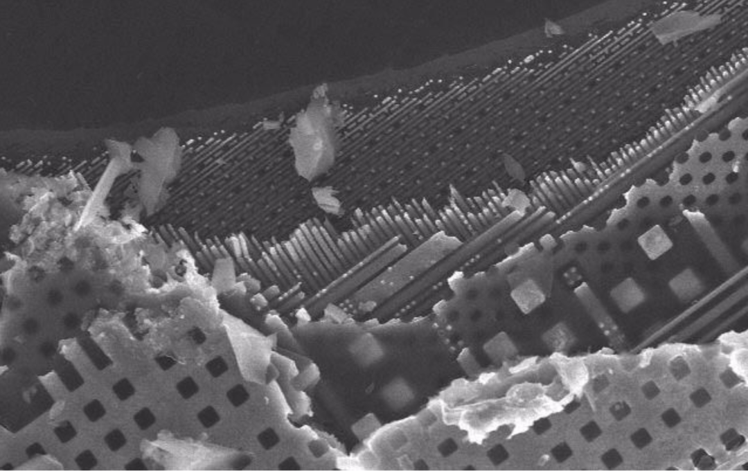
This is a top-down view SEM photo, which clearly shows the layered structure inside the CPU. The line widths become narrower as you go deeper, closer to the device layer.
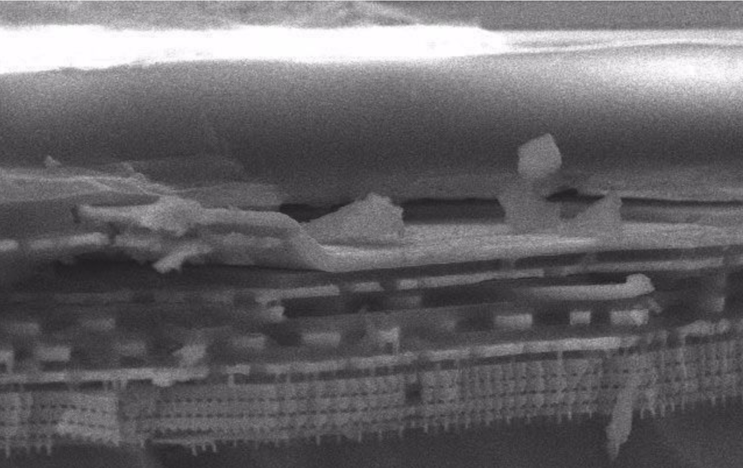
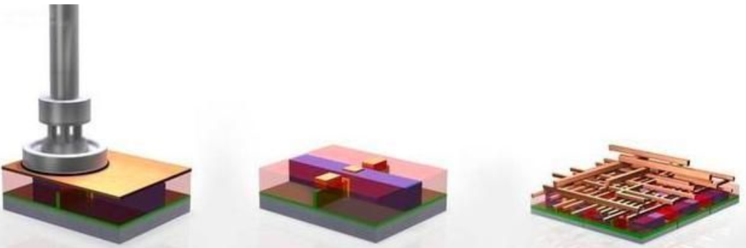
This is a cross-sectional view of the CPU, showing the layered CPU structure clearly. The internal chip uses a hierarchical arrangement, and this CPU has about 10 layers. The bottom layer is the device layer, which consists of MOSFET transistors.
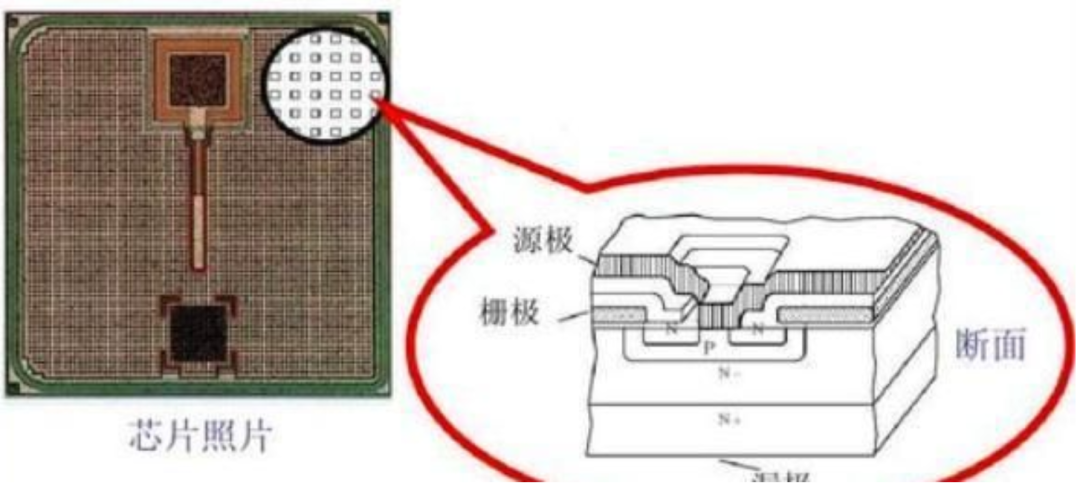
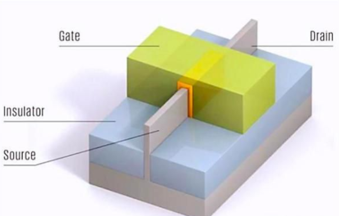
The MOSFETs in the chip can be seen as a three-dimensional structure resembling a ‘platform’. Transistors do not have inductors or resistors, which are prone to generate heat. The top layer is a low-resistance electrode, separated from the platform below by an insulator. It generally uses P-type or N-type polysilicon as the gate material, with silicon dioxide as the insulator below.
The sides of the platform are doped to form the source and drain, which can interchange their positions. The distance between them is called the channel, which determines the characteristics of the chip.
Of course, there are not only MOSFETs in the chip, but also tri-gate transistors, etc. Transistors are not installed; they are sculpted during the chip manufacturing process.
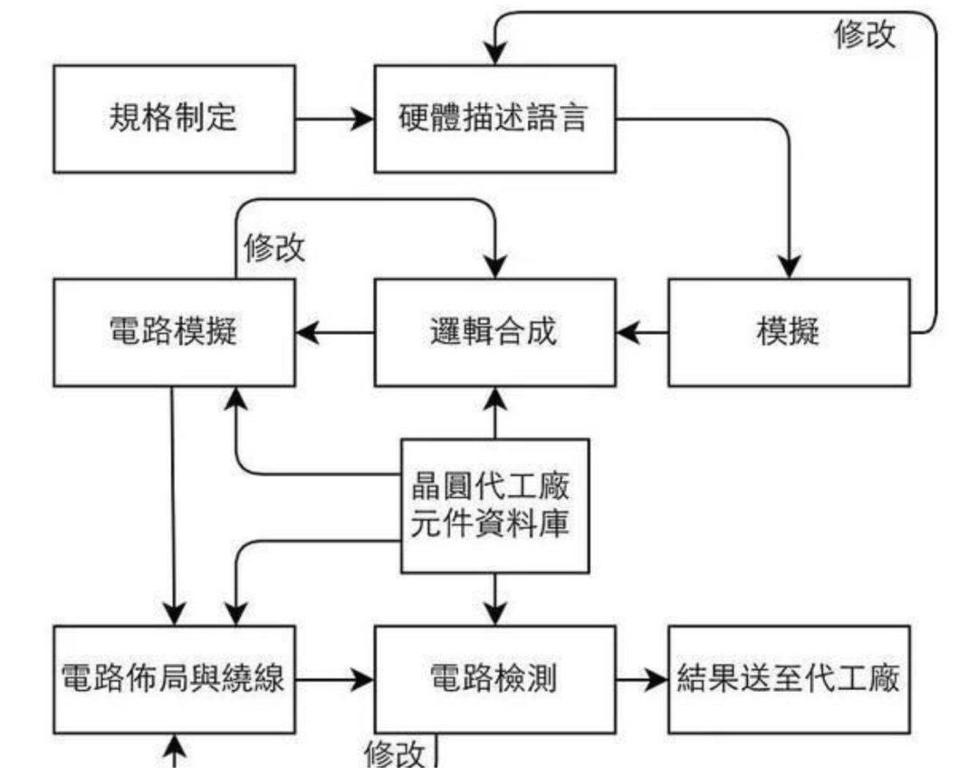
During chip design, designers use EDA tools to plan the layout of the chip and then route the wiring.
If we magnify the designed logic gate, the white dots represent the substrate, and the green borders indicate the doped layers.
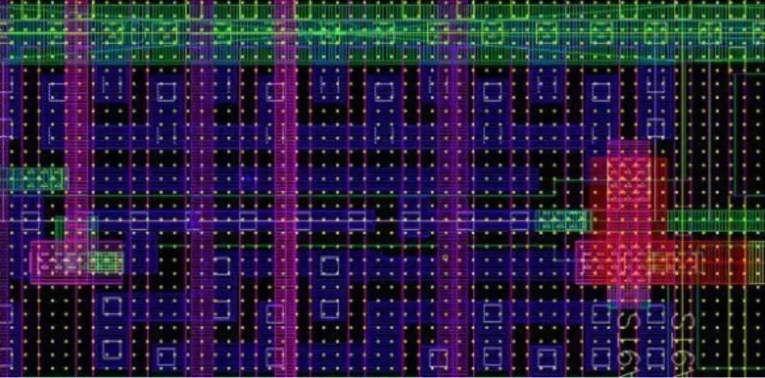
Wafer foundries manufacture chips based on the physical layout designed by the chip designers.
There are two trends in chip manufacturing: one is that wafers are getting larger, allowing for more chips to be cut out, improving efficiency; the other is the chip process, which refers to the size of the gate, also known as gate length. In the transistor structure, current flows from the Source to the Drain, and the Gate acts as a gate, mainly responsible for controlling the on-off state between the source and drain.
Current can be lost, and the width of the gate determines the loss during current flow, which manifests as the common heating and power consumption in mobile phones. The narrower the width, the lower the power consumption. The minimum width of the gate (gate length) is also called the process.
The purpose of shrinking the nanometer process is to fit more transistors into a smaller chip, preventing the chip from becoming larger due to technological advancements.
However, if we reduce the gate size, the current flowing between the source and drain will increase, making the process more challenging.
The chip manufacturing process is divided into seven major production areas: diffusion, photolithography, etching, ion implantation, thin film growth, polishing, and metallization. Photolithography and etching are the two core steps.
Transistors are sculpted through photolithography and etching. Photolithography creates the necessary lines and functional areas for chip production.
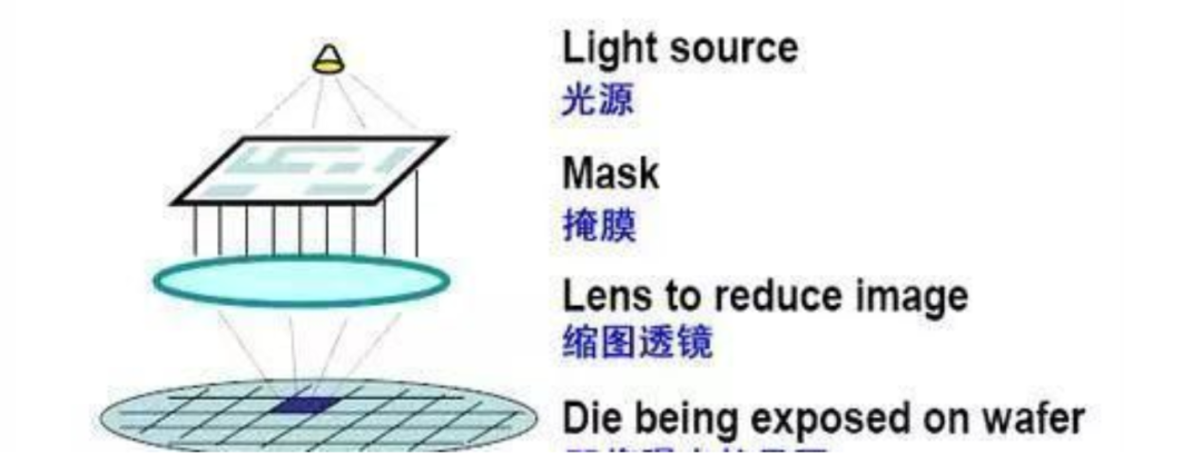
Using light emitted from a photolithography machine, the light passes through a patterned mask to expose a photoresist-coated wafer. When exposed to light, the photoresist undergoes a change in properties, allowing the pattern from the mask to be transferred onto the wafer, thus creating an electronic circuit diagram on the wafer.
This is the role of photolithography, similar to how a camera takes a photo. The photo taken by a camera is printed on film, while photolithography does not print a photo but rather a circuit diagram and other electronic components.
Etching is the process of selectively removing unwanted materials from the surface of the silicon wafer using chemical or physical methods. In the typical wafer processing flow, the etching process follows photolithography. The patterned photoresist layer does not undergo significant erosion from the etching source, thus completing the pattern transfer process. The etching step is crucial for replicating the mask pattern.
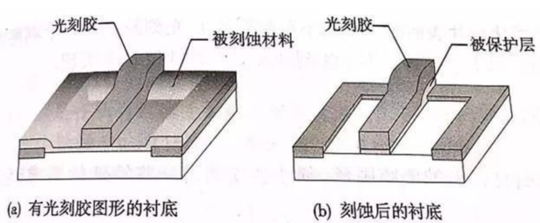
Additionally, the material involved is photoresist. It is important to know that the circuit design is first written on the photomask using lasers, and then the light source illuminates the photoresist-coated surface of the silicon wafer, causing a chemical effect in the exposed areas of the photoresist. After developing, either the exposed or unexposed areas are dissolved and removed, transferring the circuit diagram from the mask onto the photoresist, and finally using etching technology to transfer the pattern onto the silicon wafer.
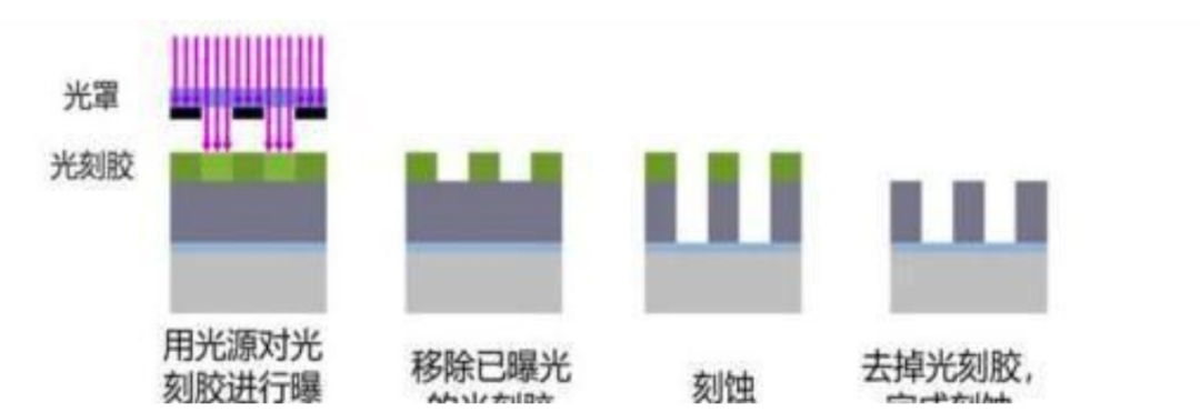
Photolithography is divided into positive and negative lithography based on the type of photoresist used, categorized into positive photolithography and negative photolithography. In positive photolithography, the exposed portions of the positive photoresist are destroyed and washed away with a solvent, making the pattern on the photoresist identical to that on the mask.
Conversely, in negative photolithography, the exposed portions of the negative photoresist become insoluble due to hardening, while the unexposed portions are washed away with a solvent, making the pattern on the photoresist opposite to that on the mask.
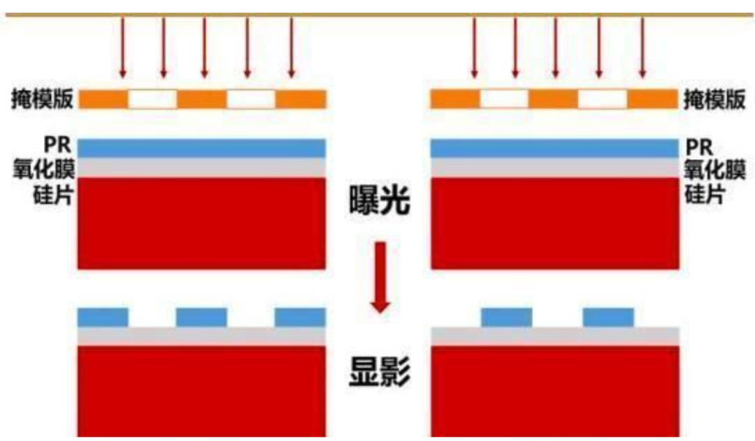
We can briefly explain this step from a microscopic perspective.
On a wafer (or silicon wafer) coated with photoresist, a pre-made photomask is placed on top, and ultraviolet light is used to irradiate the wafer through the photomask for a certain period. The principle is to use ultraviolet light to alter part of the photoresist, making it easier to etch.
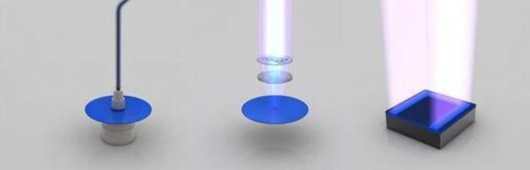
Dissolving photoresist: During the photolithography process, the photoresist exposed to ultraviolet light is dissolved, leaving a pattern consistent with the mask.
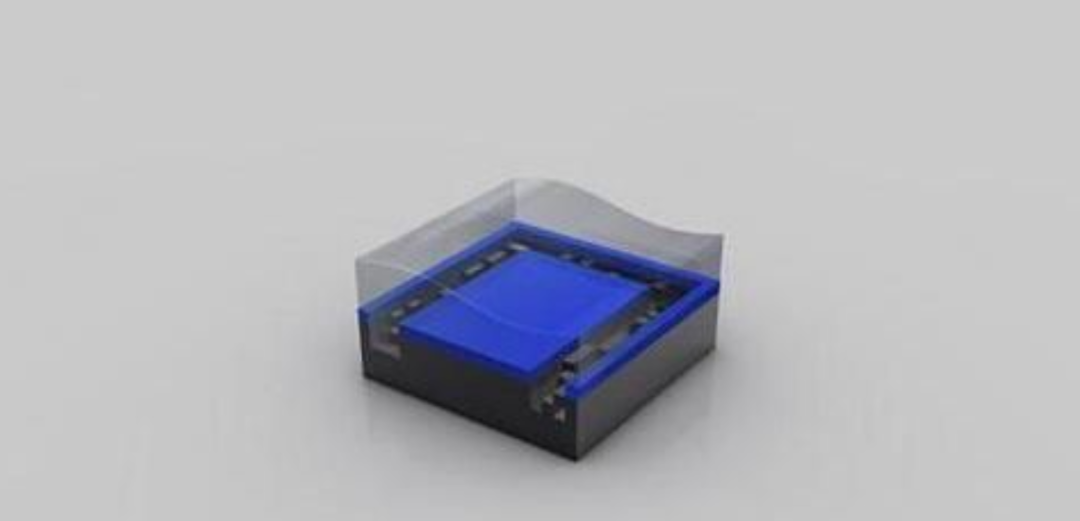
Etching is the process of using etching solution to remove the altered portions of the photoresist (positive photoresist). The surface of the wafer then reveals the patterns of the semiconductor devices and their connections. Another etching solution is used on the wafer to form the semiconductor devices and their circuits.
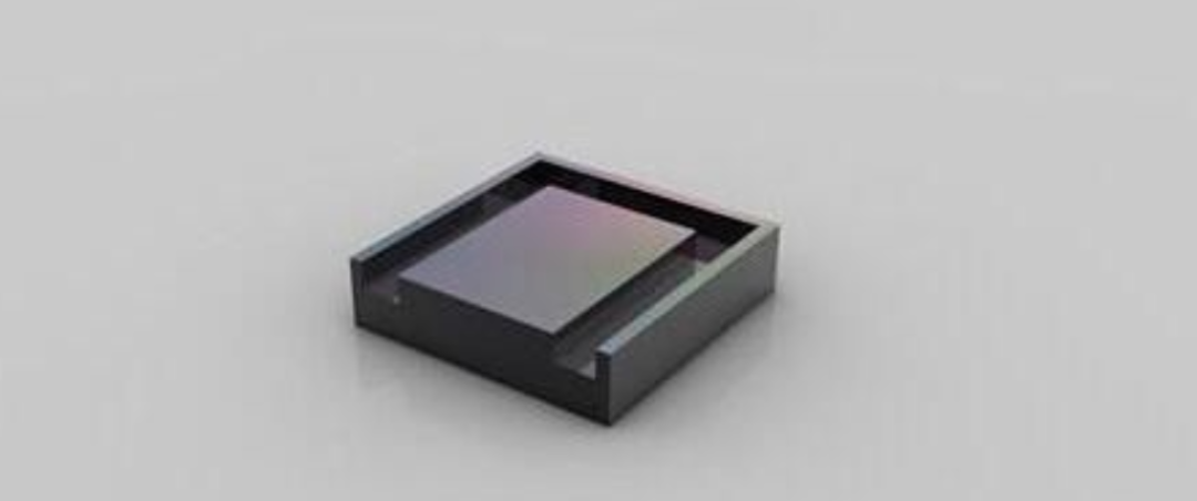
Removing photoresist: After etching is completed, the mission of the photoresist is over. Once it is completely removed, the designed circuit pattern can be seen.
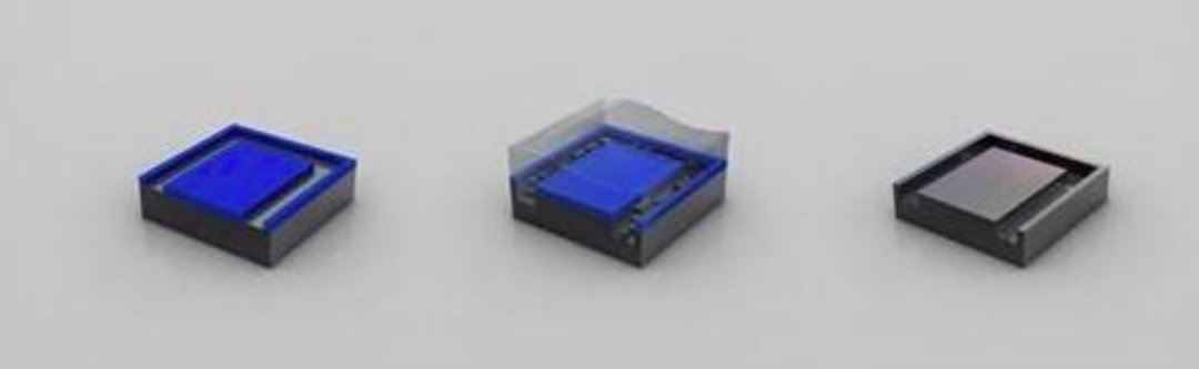
And over 10 billion transistors are sculpted in this way. Transistors can be used for various digital and analog functions, including amplification, switching, voltage regulation, signal modulation, and oscillation.
The more transistors there are, the more the processing efficiency of the processor can be increased; furthermore, reducing the size can also lower power consumption; finally, as the chip size shrinks, it becomes easier to fit into mobile devices, meeting future demands for thinness.
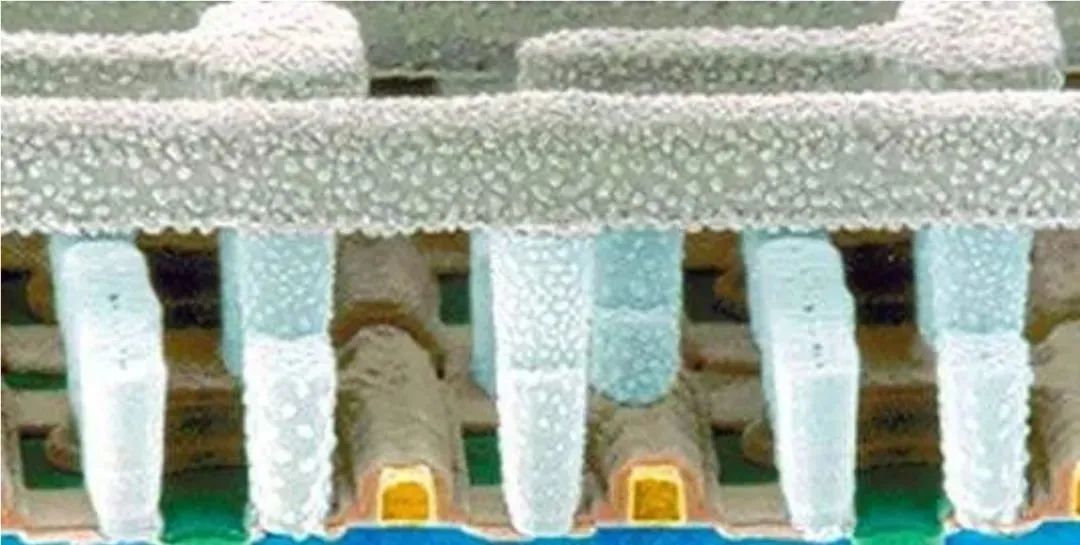
Cross-section of chip transistors
After reaching 3nm, the current transistors are no longer applicable. Currently, the semiconductor industry is developing nanosheet FET (GAA FET) and nanowire FET (MBCFET), which are considered the future of today’s finFET technology.
Samsung bets on GAA surrounding gate transistor technology, while TSMC has not yet disclosed specific process details. In 2019, Samsung was the first to announce the GAA surrounding gate transistor. According to Samsung, based on the new GAA transistor structure, they have produced MBCFET (Multi-Bridge-Channel FET) using nanosheet devices, which can significantly enhance transistor performance, replacing finFET transistor technology.
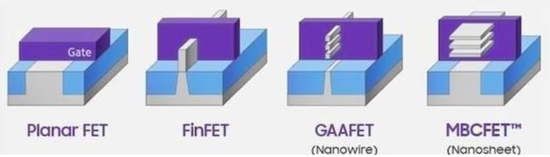
Additionally, MBCFET technology is compatible with existing finFET manufacturing processes and equipment, accelerating process development and production.
02
I found a video of TSMC’s wafer manufacturing process. Let’s take a look together.
03
This is a video explaining the process from raw materials to chip manufacturing, which is quite comprehensive. The video was shot by GlobalFoundries, a chip manufacturing plant spun off from AMD.
Source: Metal Processing, Chip Infrastructure, Manufacturing Principles, etc.