4.1 FPGA Implementation of AND and OR Logic
This section will design an AND and OR interface as shown in Figure 1.1, primarily implementing the logic AND and OR functions. The AND and OR interface includes 3 modules: clock stimulus, reset stimulus, and the AND and OR module.
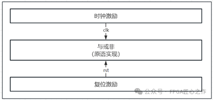
Figure 1.1 Block diagram of the AND and OR design
The functionalities of the submodules in the AND and OR interface are as follows:
1. Clock stimulus: generates 1 clock signal with a frequency of 100MHz;
2. Reset stimulus: generates a reset signal, active high;
3. AND and OR module: implements the logic AND and OR functions using logic gate primitives.
4.2 FPGA Implementation of AND and OR Stimulus
`timescale 1ns / 1ps
// Module name: test34_testbench
module test34_testbench();
wire fpga_clk_in ;// Define clock
wire sys_rst ;// Define reset
wire data_out_and ;// AND gate result
wire data_out_or ;// OR gate result
wire data_out_not ;// NOT gate result
// Instantiate test_clk module
test_clk #( .T(5))
ua_test_clk(
.sys_clk (fpga_clk_in));// Output 100MHz clock
// Instantiate test_rst module
test_rst ub_test_rst(
.sys_rst (sys_rst));// Output active high reset
// Instantiate test34_code01 module
test34_code01 u_test34_code01(
.sys_clk (fpga_clk_in ),
.sys_rst (sys_rst ),
.data_ina (1’b0 ),
.data_inb (1’b1 ),
.data_out_and (data_out_and ),
.data_out_or (data_out_or ),
.data_out_not (data_out_not ));
endmodule
4.3 FPGA Implementation of AND and OR Verification
1. Use Vivado 2019.1 software to simulate the logic gate primitives for AND and OR functions, with the simulation waveform shown in Figure 1.2. From the simulation waveform, it can be seen that the input data is a=0, b=1, and the output AND and OR results are 0, 1, 1, which meets the design requirements.
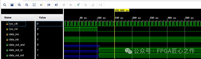
Figure 1.2 Simulation waveform of the clock generation module
4.4 FPGA Implementation of AND and OR Communication
1.It is hoped that readers can quickly learn FPGA technology;
2.It is hoped that reading the author’s public account (FPGA Craftsmanship) will be helpful to you;
3.If you need the source code, you can message the author (WeChat ID: always_fpga_study);
4.If you have any questions, feel free to message, and I will reply when I see it.