The new year’s competition has kicked off enthusiastically~
To help everyone learn more about this event, the editor has compiled excellent works from 2021 for sharing and learning.
Every Monday, we will share award-winning works, so remember to check out the series~
Team Introduction
Participating Unit: University of Science and Technology of China
Team Name: Supernova
Finals Award: Third Prize
1. Project Introduction
This design is based on the E203 processor as the core, adding co-processors, neural network accelerators, peripherals for display (12864 LCD screen and monitor connected via HDMI), input buttons, DDR, Ethernet, and other peripherals to form the SoC.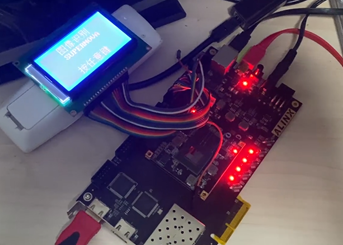
The image information to be recognized is sent from the PC to the FPGA via Ethernet and temporarily stored in DDR3. The current image to be recognized is displayed through HDMI. The accelerator retrieves the image data from DDR for recognition, offering two modes for user selection: single image recognition and continuous recognition. In single image mode, the accelerator sends the recognition result into the E203 core, and the program controls the LCD to display the corresponding characters; in continuous mode, the accelerator can return the recognition result directly to the PC host via Ethernet. The overall system architecture is shown below: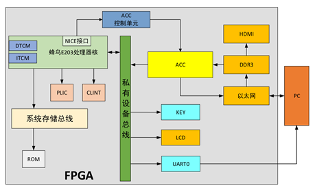
1.1 E203 Program Design
The C program mainly consists of the main function, GPIO initialization function, PLIC configuration function, GPIO interrupt function, UART configuration and sending function, and LCD control function. The flowchart of the main function is shown below. When the program is in the mode selection phase, the first GPIO button interrupt is used for mode switching, and the second GPIO button is used for mode confirmation; when the program is in selective recognition mode, the first GPIO button interrupt is used to switch the currently displayed image in mode one, and the second GPIO button is used to confirm the recognition of the current image.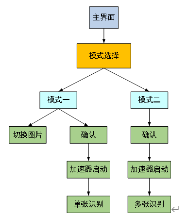
1.2 NICE Interface and Co-Processor
The neural network accelerator was designed considering two functional mode switches and low power requirements. The control of the accelerator’s start, stop, and mode selection is transmitted to the accelerator’s control module by E203 in the form of custom instructions via the NICE interface. In this system, the accelerator will directly read data from DDR; if no data is sent, it will perform invalid calculations. To reduce power consumption, we can start and stop the accelerator. Additionally, this system’s functionality includes both single image recognition and continuous recognition modes. For single image recognition, the speed requirement is not high, using a lower clock frequency, while continuous recognition is positioned for large-scale data processing, requiring higher speed, thus using a higher clock frequency. The control diagram is as follows: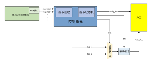
1.3 UART Communication
When the user selects a specific mode in the program, the E203 core sends the corresponding mode code to the PC via UART. The PC will then choose to send either a single image (mode one) or continuously send multiple images (mode two) to the FPGA via Ethernet. If in mode one, the program sends a command via UART to the PC to switch the current image to be recognized.
1.4 TCP/UDP Ethernet Interface
Ethernet is currently the most widely used local area network communication method and is also a protocol. The Ethernet protocol defines a series of software and hardware standards to connect different computer devices. In our design, image information is sent from the PC to the FPGA via Ethernet, and in continuous mode, the accelerator can return the recognition result directly to the PC host via Ethernet. To verify the correctness of the Ethernet interface, this article uses Wireshark software and NetAssist network debugging assistant for debugging. Wireshark can capture packets sent from the network port, allowing us to observe whether the sent packets are correct. The test results are shown below, confirming that the Ethernet functionality is correctly implemented.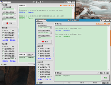
1.5 HDMI Display Image
The HDMI interface on the development board is driven by the Sil9134 chip, which requires initialization of the chip registers via the I2C communication protocol before sending image data to the screen in VGA interface timing.
1.6 LCD Display Result
For the LCD hardware module, we chose the 12864B dot matrix LCD display module, capable of displaying Chinese characters, numbers, English, and symbols.
1.7 Neural Network Model
In this design, the LCD is used to display the program’s user interface and the final recognition results from the accelerator. When the user completes mode selection and confirms recognition through the program, the accelerator begins to recognize the image under the command of the core. Upon completion of recognition, the accelerator sends the recognition result to the LCD module through the core, where the LCD module decodes the received recognition result and displays the final recognition result on the LCD screen. This design is based on the official ShuffleNet v2 x0.5 model from Megvii Technology, with some structural improvements made considering FPGA hardware resources, named ShuffleNet v2 x0.1 (hereinafter referred to as x0.1), which can classify images of 32 types of daily necessities in the ImageNet dataset. The entire model includes 5 stages, with the basic framework as follows: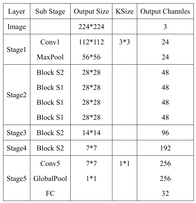 The forward inference process of this design completely uses signed integer data format for calculations, with the basic idea being to set a fixed bit width for each layer and scale the calculation results to fit within that bit width’s address range. To further save computing resources, all data scaling uses shifting operations. For weight (W) and bias (B) scaling, refer to the following formulas:
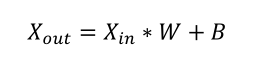 For bias (B) operations, refer to the following formulas:
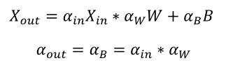 Based on the above formulas, assuming the output result of the previous layer is scaled by a ratio of 𝛼𝑖𝑛 compared to floating-point operations, and the weight scaling ratio is 𝛼𝑊, the final shift to a fixed bit width is 𝑠ℎ𝑖𝑓𝑡, the quantized integer operations will output results scaled by a factor of 𝑟𝑎𝑡𝑒 compared to normal floating-point operations, satisfying the following formula:
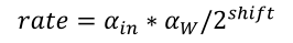 This parameter is referred to in this design as the scaling factor 𝑟𝑎𝑡𝑒. Since the scaling of the bias parameters in convolution layers requires this value and each layer’s scaling factor is different, this parameter will be passed between layers in the quantized network. Based on the above quantization strategy, after quantization inference testing of the 32 types of daily necessities selected from ImageNet, the quantized accuracy is 90%, compared to 96% accuracy in floating-point operations, which is a decline. However, considering this design uses a relatively aggressive quantization strategy (entirely integer operations and scaling using shifting operations instead of multiplication), this result is completely acceptable.
1.8 Neural Network Hardware Design
In this design, the application scenario and algorithm of the accelerator have been fixed, and the algorithm model is complex, containing multiple branches and blocks. For higher performance, we chose to implement each layer separately as the implementation method of the CNN accelerator in this SoC, then connect them to complete the entire network model. This design uses a sliding window method to generate feature maps; for generating a feature map of size 3*3, the specifics are as follows: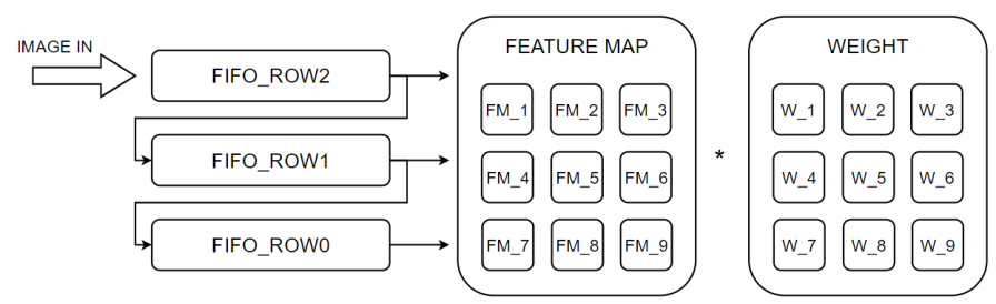
The input feature map size is 2242243, and the conv layer uses a 3×3 convolution kernel with a stride of 2 and padding of 1. The final feature map size calculated from the conv layer is 11211224. After multiplying the generated feature map with weights to obtain the calculation result, the main multiplication and addition operations are performed by DSPs, which are set to 4-stage pipelines, performing addition and multiplication operations once per cycle.
The purpose of the Shuffle layer is to shuffle the multiple channels of input data. In the FPGA, the data stream is transmitted in pixel form, so it only needs to reassemble the data according to the shuffle order. The implementation principle of the Shuffle layer is shown below: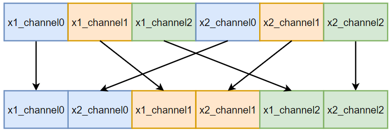
2. Technical Innovations
-
This project completed the entire process of model training, forward quantization, and hardware design, allowing for quick migration to various image classification applications based on different datasets.
-
Implemented two recognition modes: single image recognition and continuous recognition. The system is designed for cloud processing, capable of rapidly recognizing a large number of images (from Ethernet), namely continuous recognition, which achieves image data transmission and communication between the PC and FPGA.
3. Competition Experience
Through the research and exploration of this project, we learned about deep learning knowledge and embedded system construction and practice, completing the hardware implementation and performance optimization of the neural network accelerator. The system performance achieved satisfactory results. We thank the organizers for providing us with such an opportunity to enhance our practical skills and a platform for exchanging project experience.
4. Future Work
Further optimize timing and attempt to use the NICE interface to configure parameters for the accelerator (currently, the accelerator is of fixed scale and cannot be modified), optimize the PC host, etc.
Recommended Reading


【2021 Competition Work Sharing】 Issue 20 | Hardware Acceleration of SM4 Algorithm Based on E203 Processor


【2021 Competition Work Sharing】 Issue 19 | Ultra-Low Power Speech Keyword Recognition System in Adaptive Noise Environment


【2021 Competition Work Sharing】 Issue 18 | Smart Helmet Design
Source | Jishu Community
Copyright belongs to the original author. If there is any infringement, please contact for deletion.
END


About Anxin Education


Anxin Education is an innovative educational platform focused on AIoT (Artificial Intelligence + Internet of Things), providing a comprehensive AIoT education solution from primary and secondary schools to higher education.
Anxin Education, relying on Arm technology, has developed the ASC (Arm Smart Connectivity) curriculum and talent training system, which has been widely applied in university-industry-research cooperation and STEM education in primary and secondary schools, committed to cultivating talents in the intelligent interconnection field that meet the demands of the times.