Over time, the demand for digital systems and their audio data in mobile phones, computers, and home automation products has changed significantly. Audio signals sent to or from processors are gradually being digitized.
These data are processed through various devices in different systems, such as Digital Signal Processors (DSP), Analog-to-Digital Converters (ADC), Digital-to-Analog Converters (DAC), and digital input/output interfaces. To enable audio data transmission between these devices, a standard protocol is required.
The I2S protocol is one such standard. It is a serial bus interface designed by Philips Semiconductor in February 1986, specifically for digital audio interfaces between devices. This article explores an overview of the I2S protocol, its working principles, and its applications.
What is the I2S Protocol?
The I2S (Inter-IC Sound) protocol is a protocol used to transfer digital audio data from one device to another. This protocol transmits Pulse Code Modulation (PCM) audio data between integrated circuits (ICs) within electronic devices. I2S plays a crucial role in transferring pre-recorded audio files from a microcontroller (MCU) to a DAC or amplifier. This protocol can also digitize audio through a microphone. The I2S protocol does not involve compression, so it cannot play compressed audio formats like OGG or MP3, but it supports WAV files.
Features
The features of the I2S protocol include:
-
Each sample contains 8 to 32 bits of data.
-
Supports transmit (Tx) and receive (Rx) FIFO interrupts.
-
Supports Direct Memory Access (DMA).
-
Word select periods of 16, 32, 48, or 64 bits.
-
Supports bidirectional audio stream synchronous transmission.
-
Sample widths of 8, 16, or 24 bits.
-
Supports various sampling rates.
-
Data rates can reach up to 96 kHz through a 64-bit word select period.
-
Supports interleaved stereo FIFO or independent left and right channel FIFOs.
-
Tx and Rx functions can be independently enabled.
How the I2S Communication Protocol Works
The I2S communication protocol is a three-wire protocol that processes audio data through a three-wire serial bus that includes SCK (Serial Clock), WS (Word Select), and SD (Serial Data).
Three-wire connection description
1. SCK (Serial Clock)
SCK (also known as BCLK, Bit Clock) is the first line of the I2S protocol, used to synchronize data reading. Its frequency is defined by the formula:
2. WS (Word Select)
WS (also known as FS, Frame Select) is used to distinguish between the left and right channels:
-
• WS = 0: Left channel (Channel 1).
-
• WS = 1: Right channel (Channel 2).
3. SD (Serial Data)
The SD line transmits audio data encoded in two’s complement form, with the most significant bit (MSB) transmitted first. The word length at the receiver may differ from that at the transmitter:
-
If the receiver’s word length is greater than the transmitter’s, the lower bits are padded with zeros.
-
If the receiver’s word length is less than the transmitter’s, the excess lower bits are ignored.
The transmitter can transmit data on the rising or falling edge of the clock pulse (configured via control registers), but the receiver only latches data on the rising edge of the clock. The transmitter starts transmitting data after a one clock cycle delay following a change in the WS signal, while the receiver synchronizes data through the WS signal.
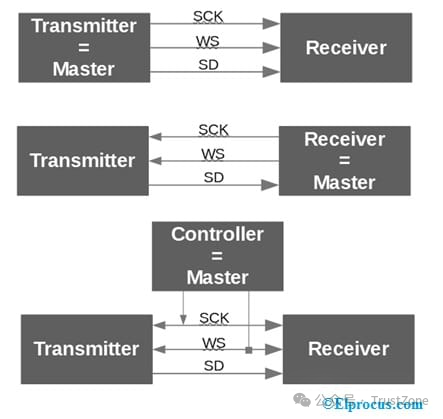
I2S Network Components
When multiple I2S components are interconnected, it is referred to as an I2S network. The components in the network are divided into master and slave devices:
- The master device is the transmitter: The master device controls the SCK and WS lines (e.g., ESP NodeMCU development board).
- The master device is the receiver: The receiver generates the SCK and WS signals.
- External master controller: An independent master device generates clock and frame synchronization signals.
Only one master device is allowed in all I2S networks, while other components synchronize data transmission based on the master device’s clock.
I2S Timing Diagram
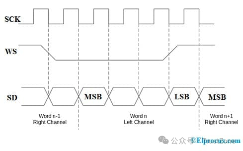
The I2S timing diagram shows the signal relationships of SCK, WS, and SD:
-
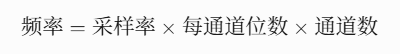
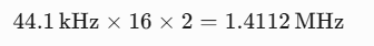
Serial clock (SCK)• Frequency formula: SCK frequency = Sampling rate × Bits per channel × Number of channels
• For example, if the sampling rate is 44.1 kHz, each channel is 16 bits, and there are two channels (stereo), then the SCK frequency is:
-
Word select line (WS/LRCLK)• Level definitions:
◦ High level (1): Right channel data transmission
◦ Low level (0): Left channel data transmission
• Timing characteristics:
◦ The WS signal switches one clock cycle before the most significant bit (MSB) is sent, providing the receiver with a buffer time:
◦ The receiver can store the current word and clear the input register, preparing to receive the next word.◦ The MSB begins transmission on the first SCK clock edge after the WS switch.
-
Serial data line (SD)• Data transmission method:
◦ Data is sampled on the falling edge of each SCK clock (from high to low), as indicated by the dots in the diagram.
Propagation delay and synchronization design
- During transmission, there is a propagation delay between the transmitter and receiver, calculated by the formula:
Propagation delay = (Phase difference between external clock and internal clock of the receiver) + (Delay from internal clock of the receiver to data reception completion)
Clock constraints to minimize delay
- To ensure synchronization between transmission and reception, the following conditions must be met:
Transmitter clock period (T):

Example parameters (transmission rate 2.5 MHz)
-
Transmitter (master device):•
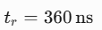
• Clock high level time (t_HC): Minimum > (0.35T)
• Clock low level time (t_LC): Minimum > (0.35T)
-
Receiver (slave device):• Clock high level time (t_HC): Maximum < (0.35T)
• Clock low level time (t_LC): Maximum < (0.35T)
• Setup time (t_su): Minimum < (0.20T)
Key notes• The above constraints ensure that the signal remains stable within the setup/hold time window at the receiver, avoiding metastability issues.
• During design, timing simulation should be performed to verify that the actual delay meets protocol requirements.
(Note: This is a technical document-level translation, retaining original formulas and parameter units, with additional comments as necessary.)
I2S Protocol and Arduino
Project example: Building a simple electronic piano (Theremin) using Arduino MKR Zero and the I2S library.
-
Components: Arduino MKR Zero, Adafruit MAX98357A I2S DAC, 3W speaker, sliding potentiometer.
-
Connections:
SD line to pin A6, SCK to pin 2, WS to pin 3.
-
Working principle: The sliding potentiometer adjusts pitch and volume, and the I2S DAC outputs a sine wave audio.
Code Example
#include <I2S.h>
const int maxFrequency = 5000;  // Maximum frequency
const int minFrequency = 220;   // Minimum frequency
const int sampleRate = 44100;   // Sampling rate
short sine[256];                // Sine wave buffer

void setup() {
  I2S.begin(I2S_PHILIPS_MODE, sampleRate, 16);
  generateSine();  // Generate sine wave data
}

void loop() {
float frequency = map(analogRead(A0), 0, 1023, minFrequency, maxFrequency);
int amplitude = map(analogRead(A1), 0, 1023, 0, 100);
  playWave(frequency, 0.1, amplitude);  // Play audio
}

void generateSine() {
for (int i = 0; i < 256; i++) {
    sine[i] = 100 * sin(2 * PI * i / 256);
  }
}

void playWave(float freq, float sec, int amp) {
unsigned int iterations = sec * sampleRate;
float delta = (freq * 256) / sampleRate;
for (unsigned int i = 0; i < iterations; i++) {
    short pos = (i * delta) % 256;
    short sample = amp * sine[pos];
    I2S.write(sample);  // Synchronous output for left and right channels
    I2S.write(sample);
  }
}
Differences Between I2C and I2S Protocols
| I2C | I2S |
|---|---|
| Used for general communication between ICs | Specifically for digital audio transmission |
| Uses two wires SDA and SCL | Uses three wires SCK, WS, SD |
| Supports multiple masters and slaves | Only one master device |
| Includes start/stop bits | No additional control bits |
| Applicable to various low-speed peripherals | Designed specifically for audio |
Advantages and Disadvantages
Advantages:
-
Separation of clock and data simplifies receiver design.
-
Supports all-digital microphone interfaces without the need for an analog front end.
Disadvantages:
-
Not suitable for long-distance cable transmission.
-
No error correction mechanism, susceptible to interference.
-
Lacks a unified connector standard.
Application Scenarios
-
Connecting digital audio devices (such as DSP, ADC, DAC).
-
Used in CD players, wireless microphones, home theater systems.
-
Data transmission between microcontrollers and audio codecs.
Conclusion
I2S is a three-wire synchronous serial protocol designed for digital audio transmission between integrated circuits. Its core function is to achieve efficient audio data stream transmission through the SCK, WS, and SD lines, widely used in consumer electronics and embedded audio systems.
I3C is an upgraded version of I2C, developed by the MIPI Alliance, combining the advantages of I2C and SPI, supporting higher speeds, lower power consumption, and dynamic address allocation.)
TDM (Time Division Multiplexing), SPI (Serial Peripheral Interface)
Transmission of Pulse Code Modulation (PCM) Audio Data
PCM has been mentioned earlier, and here is an additional note on this!
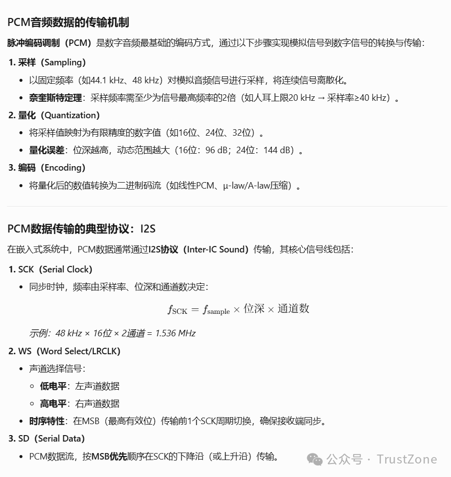
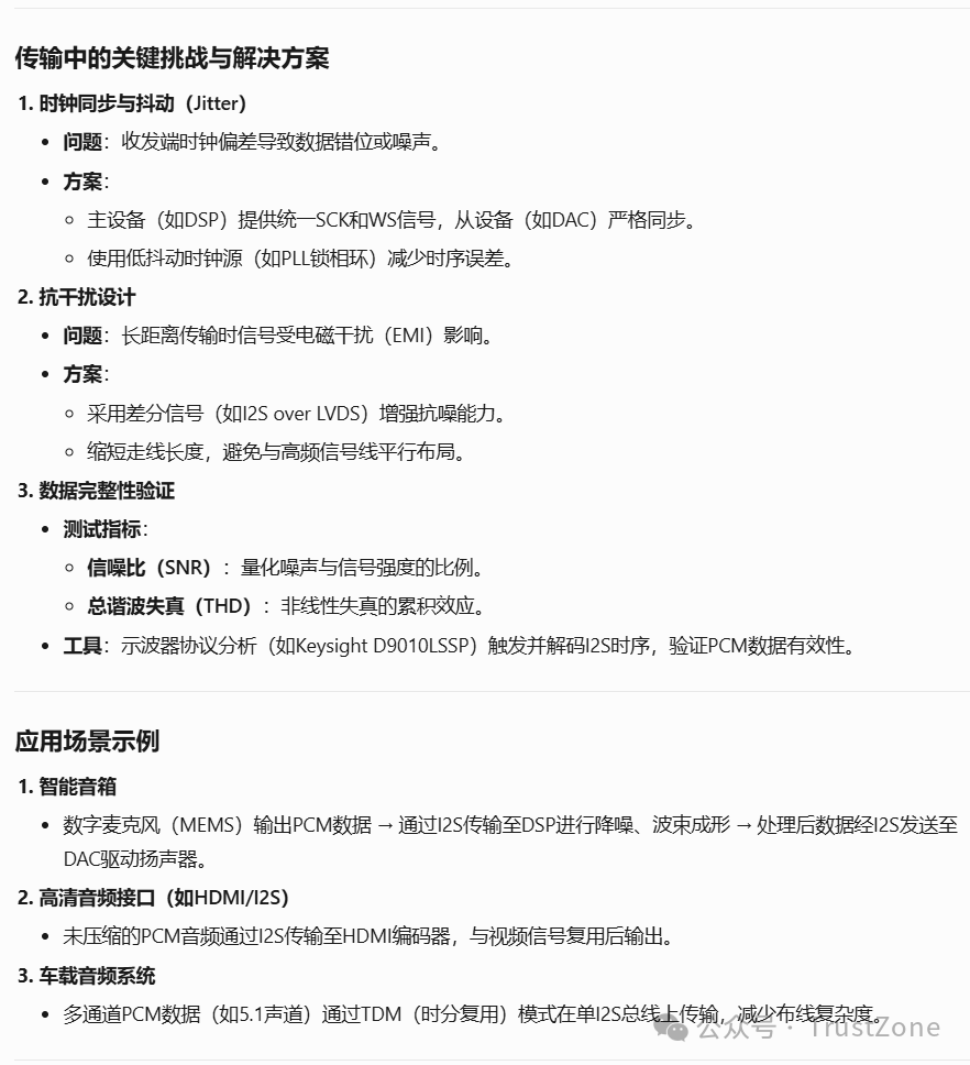
Through the above mechanisms, PCM achieves high-fidelity, low-latency audio data transmission, becoming the cornerstone of digital audio systems.