-
PLC Concept (Basic Composition, Working Principle)
-
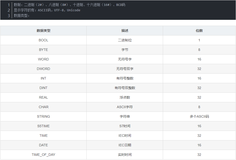
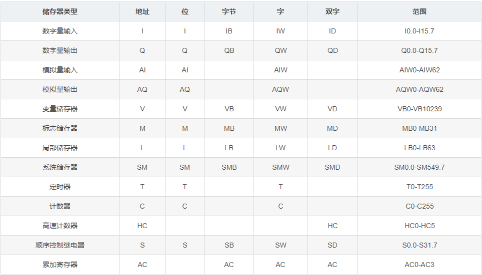
PLC Data Types & Addressing Methods (It is important to distinguish this, PLC storage size (bit, byte, word, double word BIT BYTE WORD DWORD), types of storage (Siemens DIDQAIAQMSMVLTCHTHC area; Mitsubishi XYMDTCRVZ area),
-
Data Types (INT16 DINT32 REAL STRING WORD16 DWORD32 BOOL TIME DATE CHAR8 BYTE8)
-
Types of PLC Storage (S7-200)
-
PLC System Development Process
-
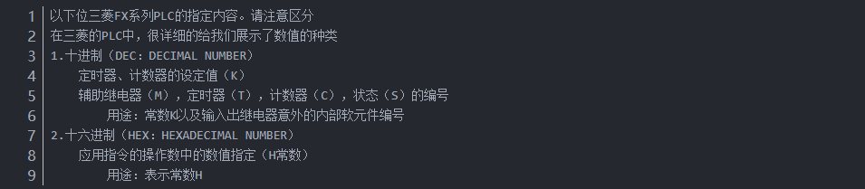
Constant Representation in PLC STEP7 (K10, H16, O8, BCD)
-
In Mitsubishi, D0 is 16 bits, two bytes. M0 is 1 bit.
-
In Siemens 1200, all are M area, represented by MB/MW/MD for 8-bit, 16-bit, and 32-bit
-
In Siemens 200 smart and 200, all are V area
PLC (Programmable Logic Controller), a computer used for industrial control.
Basic Composition of PLC
The basic composition includes power supply, CPU, memory, input unit, output unit, communication interface, expansion interface.
(1) Power Supply: The PLC can be powered by 220VAC or 24VDC, and the power required for the CPU processing unit is 5VDC.
(2) CPU (Central Processing Unit), which includes the controller, arithmetic unit, and registers.
(3) Memory is a semiconductor circuit with memory function, capable of storing system programs, user programs, and logical variables. It is divided into ROM (Read Only Memory system storage area) and RAM (Random Access Memory).
i. The ROM storage area is divided into system management programs, user program editing, instruction interpretation programs, subroutine calls, and management programs.
ii. The RAM storage area includes user program storage area and data storage area, used to store user programs and ON/OFF status quantities of various points during program execution. The data in the user storage area is readable and writable. The materials used are CMOS RAM or EPRAM and EEPRAM. The capacity is generally measured in “words” (16 bits for 1 word, 8 bits for 1 byte). Therefore, it is recommended to use even-number programming during programming.
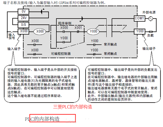
(4) The input unit refers to the unit that receives signals, detects the information sent by signals, and converts it into digital signals of high and low levels. (Divided into digital and analog signals, analog signals usually use A/D conversion circuits to convert analog signals into digital signals. The digital signal uses many interface circuits, divided into internal DC input (12V or 24V), external AC input (100-120V, 200-240V), external AC and DC input, and input circuits connected to signal output.) (AC input, DC input, source type, leakage type, common cathode, common anode, external signal output connected to PLC input unit (PNP, NPN))
(5) The output unit refers to converting weak electrical signals processed by the CPU into level signals. (Level signals refer to the power ratio of device output signals to input signals, usually expressed as P, where P=lgP2/P1.) (Output interfaces are divided into digital and analog signals. Analog signal interfaces usually use D/A conversion circuits to convert digital signals into analog signals, and digital output circuit forms are diverse, including relay output, transistor output (PNP, NPN), and thyristor output.)
(6) Communication interfaces implement communication with monitors, printers, other PLCs, computers, and other devices.
(7) Expansion interfaces add some special function modules to the PLC, such as high-speed counting modules, closed-loop control modules, motion control modules, and interrupt control modules.
Working Principle of PLC
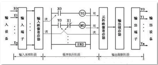
PLC Power On → Internal Processing → Communication Processing → Self-Diagnosis → Input Sampling → User Program Execution → Output Refresh
PLC adopts a cyclic scanning method, centralized input, and centralized output.
The advantages are: high reliability and strong anti-interference ability. The disadvantages are: slow response speed and response lag. PLC uses WDT (watchdog timer) to monitor whether the scan exceeds the preset time.
Internal self-processing: includes hardware initialization, I/O module configuration check, power-off protection range setting, etc. In the self-diagnosis testing phase, the CPU checks the status of each PLC module, and if an abnormality occurs, it immediately performs diagnostics and processing, while providing a fault signal and lighting up the LED indicator on the CPU panel. When a fatal error occurs, the CPU is forced into STOP mode, halting program execution. The CPU’s self-diagnosis test will help to detect or predict system faults in a timely manner, improving system reliability.
During the communication processing phase: the PLC communicates with intelligent modules equipped with its own CPU and other external devices, completing data transmission and reception, responding to commands from the programmer, updating the content displayed on the programmer, and updating the clock and special register contents. In the communication processing phase, the CPU checks for communication tasks; if there are any, it calls the corresponding process to complete communication processing with other devices (e.g., intelligent modules with microprocessors, remote I/O interfaces, programmers, HMI devices, etc.) and processes the communication data accordingly.
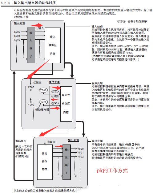
(Self-diagnosis → Input Sampling → User Program Execution → Output Refresh →) constitutes one scanning cycle.
Input sampling phase: scans all input terminals and stores their states (0/1) in the input register (PII). Then, it closes the input channel and proceeds to the next program step. This method is highly reliable but may have a certain time delay. In large projects, due to time constraints, periodic input sampling, direct input sampling, interrupt input sampling, and intelligent I/O interface module sampling may be adopted to improve speed.
User program execution phase: during this phase, data from the input register (PIQ) and internal component registers (internal relays, counters, timers) are extracted, and based on logical and arithmetic operations in the program, results are written to the output image register and related memory. Therefore, within the PLC, the state of internal component registers is constantly changing.
Output processing phase: after the program execution is completed, all output relay states in the internal component registers are transferred to the output latch in one go during the output phase, which is then delivered to the output end through isolation and driving power amplification circuits, driving the actual load connected to the external PLC wiring.
Input-output lag time: this time is also known as system response time, including input circuit filtering time, output circuit lag time, and lag time caused by scanning work methods. The response delay of PLC is generally several milliseconds to tens of milliseconds, which does not affect general systems. If a shorter response time is required, we can use PLCs with faster scanning speeds or take measures such as interrupts.
(1) Input circuit filtering time. This is mainly due to external signals possibly containing noise interference, voltage spikes, and external jitter affecting our input signals. Therefore, RC filtering circuits (composed of voltage sources and current sources driving capacitors and resistors) and optocouplers (using optocouplers on the input side to isolate internal and external electrical connections) are used to eliminate these effects. The time constant of the filtering circuit determines the length of the filtering time.
(2) Output module circuit lag time: this is related to the type, with relay output module lag time generally being 10ms, bidirectional thyristor lag time being 1ms-10ms, and transistor lag time being less than 1ms.
(3) Lag time caused by the scanning work method: it can be as long as 2-3 scanning cycles.
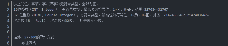
Data processing inside the hardware is performed in binary.
Negative number processing is also implemented using the binary complement.
Usage: internal processing.
In the Mitsubishi FX series, the soft component numbers for input relays and output relays are X0~X7 Y010~Y017.
Usage: soft component numbers for input and output relays.
BCD code represents decimal numbers in binary form; for example, the BCD code for 10 is 0001 0000.
Usage: BCD numerical switches, 7-segment display.
In the Mitsubishi FX series, binary is used for real number calculations, and decimal is used for real number monitoring.

String constants can be up to 32 bits.
Character length is 8 bits, so D100 (16 bits) can represent two characters.
The string data starts from a specified position (either D100 or M100), and when it encounters the OOH code (which is the NULL code, requiring 16 bits), it indicates the end of the string. If it does not encounter OOH or only encounters general codes, it will not detect the end of the string.
In the Mitsubishi FX series, the number of bits is designated as (KnX0 ………).
Bit soft components are those that process ON/OFF information.
Soft components like T, C, D, R that process numerical information are word soft components.
However, our bit soft components can also be used as words through combination. The bit number Kn and the starting soft component number of 4-bit units, K1K4 indicates 16 bits; K1K8 indicates 32 bits.
Continuous word designation.
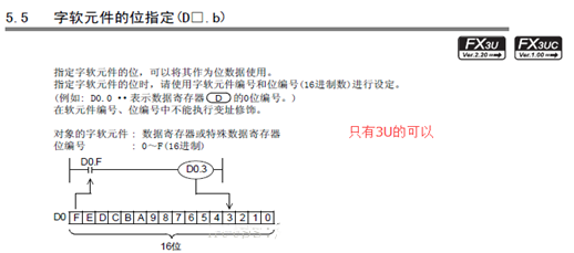
Sub soft component bit designation (D100.E).
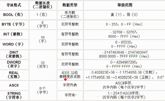
(Bit (BOOL) → Byte (BYTE) → Word (WORD)/Integer (INT) → Double Word (DWORD)/Double Integer (DINT)/Floating Point (REAL))
ASCII/String (STRING)
1 TTL level signal is 1 bit; 8 bits make 1 byte; 2 bytes make 1 word; 2 words make 1 double word.
Bit is BOOL, Boolean type, range is 0 / 1.
Byte range is 0—255; 0-FF; adjacent 8 bits are (0-7) (IB1=I1.0~I1.7).
Word range is 0—65535; 0000-FFFF; adjacent two bytes (IW2=IB2+IB3).
Double word range is 0—2^32; 00000000-FFFFFFFF; adjacent two words (ID4=IW4+IW6=IB4+IB5+IB6+IB7).

Addressing methods include bit addressing, byte addressing, word addressing, and double word addressing.
Bit addressing: I0.0 I0.1 I0.2 I1.5 I2.7 I2.8 (error)
Byte addressing: VB0 VB1 VB2 VB3… (interval of 1)
Word addressing: VW0 VW2 VW4 VW6 VW32… (interval of 2)
Double word addressing: VD0 VD4 VD8 VD32…. (interval of 4)
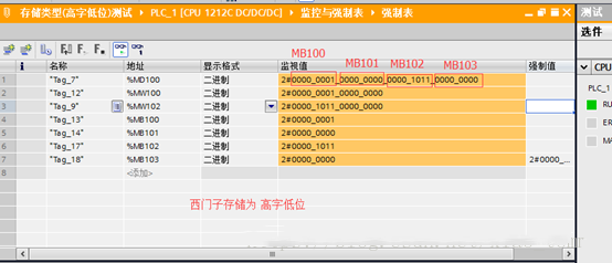
How to understand Siemens data storage types as high word low bit?
MD100
MW100MW102
MB100MB101MB102MB103
M100.7/6/5/4/3/2/1/0M101.7/6/5/4/3/2/1/0M102.7/6/5/4/3/2/1/0 M103.7/6/5/4/3/2/1/0
Among them, M103.0 is the low bit of the high byte; M100.7 is the high bit of the low byte.
Mitsubishi’s data storage type is high word high bit, how to understand? (Storage increases from right to left)
D100
D101D100
D101. F/E/D/C/B/A/9/8/7/6/5/4/3/2/1/0D100.F/E/D/C/B/A/9/8/7/6/5/4/3/2/1/0
Among them, D101.F is the high byte’s high bit; D100.0 is the low byte’s low bit.
①
Immediate addressing
②
Direct addressing
a) Absolute address
b) Symbolic address
③
Indirect addressing
a) Memory indirect addressing
i. 16-bit pointer (DB, T, C)
ii. 32-bit pointer (memory indirect addressing)
b) Register indirect addressing
i. 32-bit pointer internal addressing
ii. 32-bit pointer memory cross-addressing
V memory (variable memory) is generally used to store intermediate logical results, very common.
M memory (flag memory) is generally used for marking. Not commonly used. MB0-MB13 stores these 14 bytes.
Stored permanently in EEPROM, maintained permanently during power off.
SM memory (system memory): can be viewed in F1 help, or in the WIN symbol table for S7-200 instructions.
SM0.0: This bit is always on.
SM0.1: Turns on during the first scan, used for initializing programs.
SM0.5: Clock pulse, closed for 0.5s, open for 0.5s.
L storage area (local storage area): V storage area is globally valid, while L storage area is only locally valid. The local storage area requires dynamic allocation by the CPU, and when an interrupt program or a subroutine is called, the CPU allocates local memory to the interrupt program or subroutine. Additionally, local storage must be initialized during allocation since the data provided is random.
AC registers (accumulator registers): can pass parameters to subroutines and store intermediate calculation results. S7-200 provides four 32-bit accumulators (AC0, AC1, AC2, AC3).
By the way: The registers in S7-300 include: ACCUx accumulators, AR1/AR2 address registers, data block registers, status words.
The storage areas in S7-300 include: I/Q input/output process image area, M (bit storage area), T timers, C counters, PQ/PI immediate access output/input modules, DB shared data blocks, DI background data blocks, L local data.
(1) Clarify system control requirements.
The system requires three buttons to control forward, reverse, and stop, and requires overload protection for the motor, as well as self-locking and interlocking for forward and reverse.
(2) Identify input and output devices and assign corresponding I/O terminals.
(3) Draw the system control circuit diagram.
Main circuit, control circuit.
(4) Write the PLC control program.
Forward control, reverse control, stop control, overload protection.
(5) Program debugging.
(6) Install the system control circuit and conduct on-site debugging.
After debugging the program, on-site debugging follows. (Hardware issues & software issues)
(7) System put into operation.
Trial for a period.
In STEP7, constant values can be bytes, words, double words, and the CPU stores constants in binary. In STEP7, constants can also be represented in decimal, hexadecimal, ASCII code, floating-point, and other formats.
B#W16, W#16#, DW#16# represent hexadecimal byte constants, hexadecimal word constants, and hexadecimal double word constants.
2# represents binary constants.
L# represents 32-bit double integer constants.
P# represents address pointer constants.
S5T# represents 16-bit S5 time constants.
T# represents signed 32-bit IEC time constants.
DATE is the ITC time constant.
C# represents 16-bit counter constants (BCD code).
ASCII characters are represented using single quotes ” and each ASCII code occupies one byte.
When entering constants, be sure to use English punctuation.