
Power consumption is a critical performance metric in chips, sometimes even determining the success or failure of a chip. As is well known, the recent “Snapdragon Fire Dragon” incident significantly impacted the market share of this chip. For industrial-grade and automotive-grade chips, the impact of power consumption is not very apparent. However, for consumer-grade chips (such as mobile phone CPUs, IoT chips, etc.), low power design becomes particularly important due to their application in small mobile devices.
Industry experts have pointed out that the effectiveness of power optimization varies at different design levels. The table below shows the percentage of power reduction that can be achieved at different stages of a product’s lifecycle.
| Design Level | Power Reduction Percentage |
| Layout Level | <5% |
| Transistor Level | 5% |
| Gate Level | 10% |
| RTL Level | 20% |
| System Level | >50% |
From the chip level, methods to reduce power consumption can be approached from both process and design aspects. Process optimization is something that fab engineers need to consider, while as a chip developer, the focus is primarily on the design level. The main methods for reducing power consumption from the design perspective include: implementing clock gating and parallel module design.
Introduction to Clock Gating
Generally speaking, the clock tree runs throughout the chip and consists of numerous buffers and inverters. The clock signal, being the signal with the highest toggle rate in the chip, can account for up to 30% of the total chip power consumption, or even more. By adding clock gating (cg) circuits, the toggle behavior of the clock tree can be significantly reduced, thereby lowering switching power consumption. Additionally, the reduction in clock pin switching behavior will also decrease the internal power consumption of registers.Clock gating is a powerful means to reduce power consumption. When the clock is gated off, the clock network and the registers within it will stop toggling, resulting in a significant reduction in power consumption. A typical clock gating design is shown in the figure below:
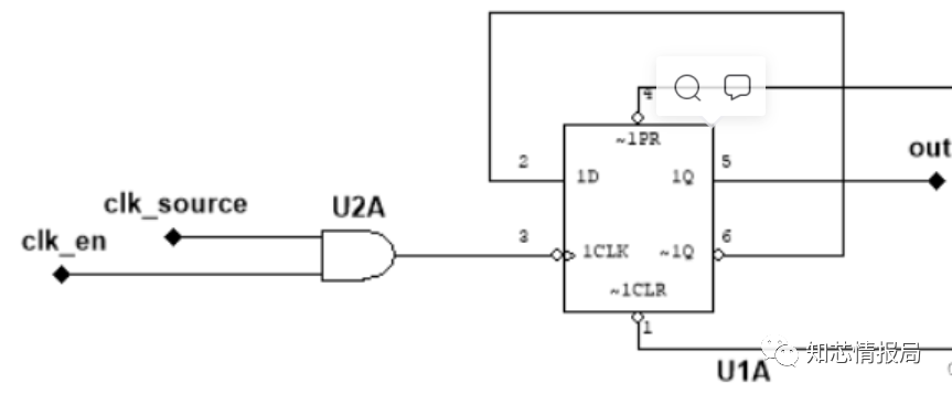
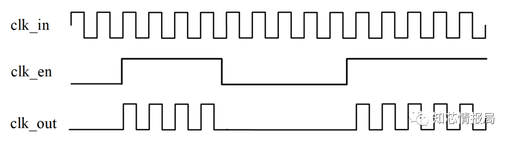
For the clock source clk_source passing through an additional AND gate U2A, when clk_en is high, clk_source can reach the U1A flip-flop; when clk_en is low, clk_source cannot reach the flip-flop. When clk_en is low, the flip-flop and all combinational logic in its clock network stop toggling, and the output remains unchanged. Since clk_source passes through the U2A AND gate, there will be some clock skew. In waveform analysis, the following diagram can better illustrate the concept of clock gating: only when clk_en is high does clk_out=clk_in; otherwise, clk_out=0.
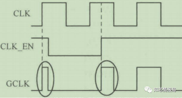
cg Method 1: Using AND Logic
This is also the simplest method,directly combining the clock enable control (gating) signal with the clock using AND logic. This method is straightforward but has a significant drawback: it can produce glitches. When clk is low, clk_en can change arbitrarily, and gclk remains low. However, when clk is high, clk_enmust remain unchanged to ensure there are no glitches. So, what can keep clk_en unchanged? The answer is:a latch
cg Method 2: Adding a Latch
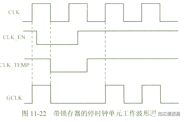
When clk is low, the latch is connected; when clk is high, the latch locks, as shown in the figure below: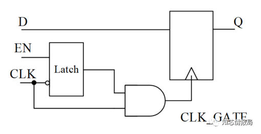 The waveform diagram below shows that when clk is low, gclk remains low, but when clk is high, the value of gclk can be considered as the clk_en value sampled at the rising edge of clk. Therefore, using a latch can effectively store the clk_en value without affecting the periodicity of clk. The essence of latch clock gating is that the rising edge of clk locks the clk_en value, preventing clk_temp from toggling when clk is high, thus eliminating glitches.
The RTL code is as follows:
always@(*) begin if(clk) clk_temp = clk_en; else clk_temp = clk_en;endassign gclk = clk & clk_temp;cg Method 3: Using Standard Cell Libraries
Although using a latch can solve the issue of glitches in clock gating, timing constraints must also be strictly enforced.When designing FPGA or ICs, the synthesis library often includes integrated clock gating logic cells. These clock gating logic cells have undergone extensive updates and validation, making them more convenient and safer to use.Therefore, in general, clock gating designs will directly call specialized integrated clock gating logic cells. The invocation method is similar to that of basic cells like AND gates and buffers; they can be instantiated directly.
The content of this article represents the author’s views and does not reflect the views of the platform.
If there are any objections, please feel free to contact us.
If there is any infringement, please contact us for deletion.
PreviousHighlightsReview
The first snow of 2021! Interpretation of Intel’s Q4 2020 financial report
Firmware compression can achieve lower energy consumption and faster boot in IoT devices

Technological advancements in core IP accelerate innovation in satellite navigation chips

The semiconductor law is gradually becoming invalid, so what does the future hold for processors?