Welcome FPGA engineers to join the official WeChat technical group.
Clickthe blue textto follow us at FPGA Home – the largest pure FPGA engineer community in China
For FPGA debugging, we mainly take Intel FPGA as an example, simulating and debugging in the Win10 Quartus II 17.0 environment, using the development board type EP4CE15F17. This mainly includes the following parts:
– FPGA Debugging – Virtual JTAG (Virtual JTAG) – FPGA Debugging – In-system Memory Content Editor – FPGA Debugging – Embedded Logic Analyzer (SignalTap) – FPGA Debugging – LogicLock – FPGA Debugging – Guidelines for Debugging Designs. The above content mainly refers to “Communication IC Design”; those interested can purchase the book for study.
1. Related Theoretical Knowledge1.1 Embedded Logic Analyzer
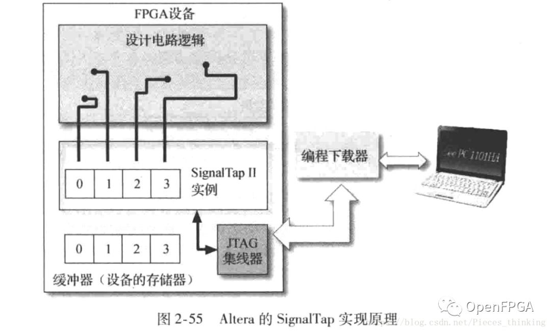
To facilitate user debugging, FPGAs typically have built-in signal observation logic. Altera provides SignalTap, while Xilinx offers ChipScope. Additionally, there are third-party debugging tools, such as Synopsys’s Identify. The core principle of these tools is to sample the internal signals or pin states of the FPGA in real-time at a pre-set clock rate and store them in the FPGA’s internal RAM, then analyze and manage the data through a unified ELA (Embedded Logic Analyzer). When the preset trigger conditions are met, the ELA uses JTAG to transfer the cached data stored in the on-chip RAM to the PC. Once the PC receives the JTAG returned data, it processes it locally to display the corresponding logic analysis results.

Therefore, whether it is SignalTap or ChipScope, they essentially add some special modules in the project to achieve signal acquisition, with costs including: logic units, internal RAM, and ELA resources. The data capture principle of the logic analyzer is shown in Figure 2-53; all storage units share RAM with the current logic design. If the current logic occupies a large amount of RAM, the embedded logic analyzer function will have a significant storage depth limitation.

From Figure 2-53, it is easy to see that the timing of logic triggering can be dynamically adjusted, and the length of stored data can also be easily adjusted. Furthermore, due to the FPGA’s built-in programmability, trigger conditions can depend on other event triggers, allowing for multi-level triggering and state-based data capture.
For example, when signal A is high for 32 cycles, if signal B is low and signal C has a low pulse, a wait event is triggered; after 65536 clock cycles of waiting, data is captured and sent out through the logic analyzer. This is a state machine-based triggering logic analysis function, akin to a combination of assertions in Verilog and FSM state machines, which traditional logic analyzers cannot achieve. As modern logic tends to be quite complex, traditional conditional triggering methods often consume time and effort, making it difficult to quickly find bugs; state-triggering often helps designers quickly locate errors and debug.
For the logic analyzer, in addition to trigger conditions, there is also a concept of storage location. Under normal circumstances, the FPGA will continuously sample the required data. When the data fills up, it will use a circular overwrite method for storage, similar to the wrap concept in FIFO. When the trigger is activated, the buffer is usually full; if pre-triggering is used, it will continue to record 12% of the current storage capacity before stopping (some vendors stop recording and use the current recorded data directly); if post-triggering is used, it will continue to record 88% of the current storage capacity before stopping (some vendors record the entire capacity); if mid-triggering is used, it will continue to record half of the current storage capacity. In fact, when to start recording and when to stop can be implemented through state triggering. A conceptual diagram of data capture is shown in Figure 2-54.
Next, we will use SignalTap as an example to briefly discuss debugging techniques for embedded logic analyzers.
1.2 SignalTap
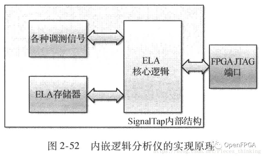
SignalTap is Altera’s built-in logic signal observation tool, with an internal implementation structure as shown in the figure.
Based on the previous principles of the logic analyzer, it is easy to know that FPGA can implement multiple parallel ELAs. By supporting multi-level triggering through FSM and conditional judgment, FPGAs can also support complex state machine data capture. Adding a counter to the trigger conditions makes it easy for the FPGA to capture data at different starting times. The SignalTap designed by Altera is designed in this way, with the following characteristics:
-
Supports up to 1024 data capture channels
-
A single device supports multiple concurrent logic analysis modules, including signals across multiple clock domains
-
Each data capture channel can support 10 levels of triggering
-
Supports capturing at different positions, including the front, middle, and back of the signal. The capture process of SignalTap is shown in the figure.
 1.2.1 SignalTap Interface
The operational interface is shown in the figure.
 1.2.2 SignalTap Demonstration
The demonstration is included in the examples.
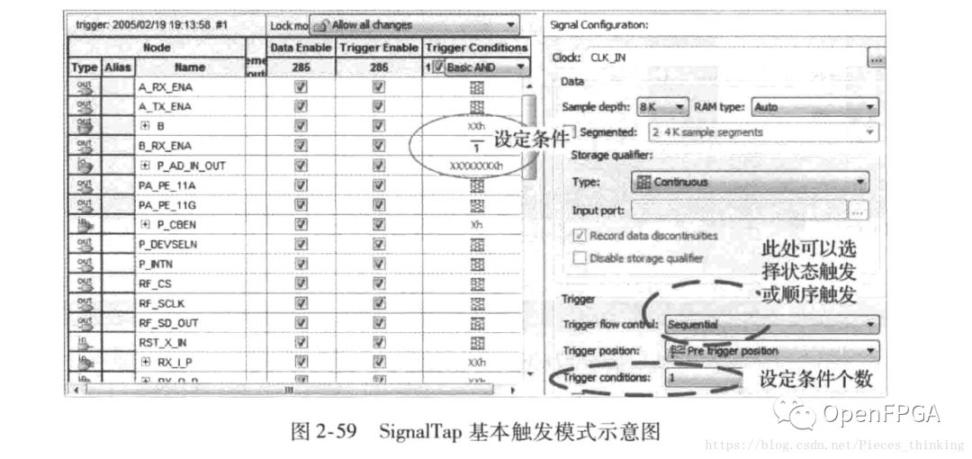
1.2.3 Basic Trigger Modes of SignalTap
When the logic analyzer is activated, SignalTap continuously samples the monitored signals until a certain condition is met to stop, which is the trigger condition. In the basic mode, the trigger condition is set as the logical combination of the current signals. When the logical combination meets a certain value, the trigger condition will be satisfied, and the data will be sampled, saved, and uploaded to the PC.
The following figure shows the basic trigger mode of SignalTap.
 1.2.4 Advanced Trigger Mode of SignalTap
In the Trigger Conditions field of the signal list, select Advanced at the top; this will pop up the logic editor, where a complex trigger expression can be designed.
1.2.5 State-Based Trigger Mode of SignalTap
The state-based triggering logic analyzer mode is the core technology of the embedded analyzer in the FPGA; the main technique is to implement state machine triggering through any state trigger statements. The following figure shows the working interface of state machine triggering.
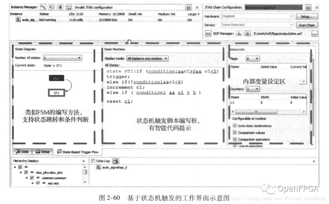
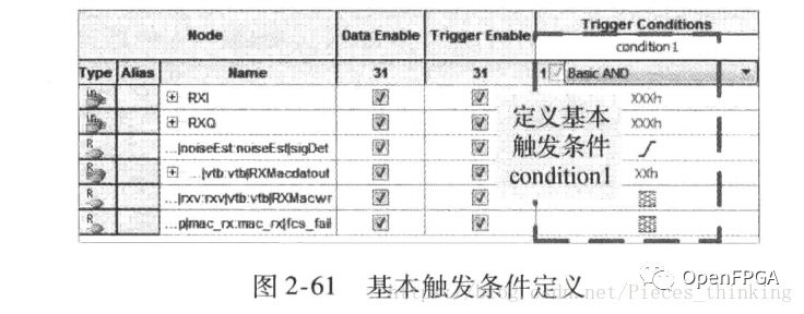
Before setting the trigger conditions, the basic trigger conditions need to be determined, as shown in the figure.
After setting the basic trigger conditions, the state machine script design can be activated. Below are a few examples to illustrate the implementation of state machine triggering:
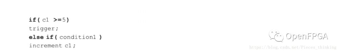
1) When condition condition1 is not met, and the duration exceeds 5 clock cycles, trigger the trigger; the ideal waveform is shown in the figure:

The corresponding state machine triggering code is as follows:
2) When condition condition1 is not met, and the non-meeting condition occurs within 5 clock cycles, and then condition condition1 is met, trigger the trigger; otherwise, stop triggering. A typical example is shown in the figure below.
The script for the above trigger is as follows:

3) When condition condition1 is met 5 times, trigger the trigger; otherwise, stop triggering. The script for this example is as follows:

4) When condition condition1 is met, if condition condition2 can be met, trigger the trigger immediately; otherwise, stop triggering. The script for this example is as follows:

5) When condition condition1 is met, if condition condition2 can be met within 5 sampling clock cycles, trigger the trigger immediately; otherwise, stop triggering. The script for this example is as follows:

Since any complex condition can be simplified into three situations: sequence, branch, and loop, counters can implement loops, conditional judgments can achieve branches, and state machines can implement process control. Therefore, any complex condition triggering can be captured through the above condition combinations.
The five examples mentioned earlier are combinations of the above different scenarios, so readers only need to combine the five examples to grasp the implementation of trigger conditions and proficiently carry out FPGA debugging.
2. Simple Example2.1 Create a New Project
First, create a new project, then add files. The content of the file is as follows:
module test ( input CLOCK, RESET, output [7:0]oData );

 reg [7:0]C1;

 always @ ( posedge CLOCK or negedge RESET )
 if( !RESET )
 C1 <= 8'd0;
 else if( C1 == 32 -1 )
 C1 <= 8'd0;
 else
 C1 <= C1 + 1'b1;

 assign oData = C1;

endmodule
The logic is very simple. Here, CLOCK is the clock pin, RESET is the reset pin, and the function of this module is to continuously count and output the count via Data. Next, after synthesis and pin assignment, we can set up SignalTap.
1.2 Configure SignalTap II Logic Analyzer
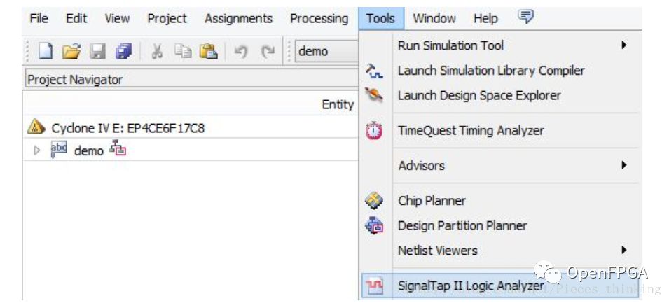
As shown in the figure, click the Tool menu, then select SignalTap II Logic Analyzer to activate the tool.

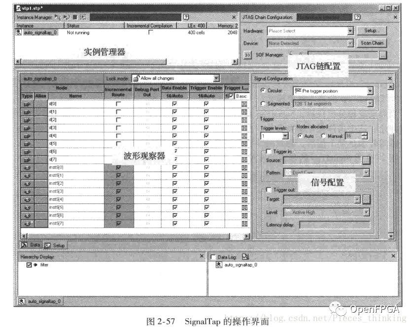
The following figure shows the SignalTap window, where the four highlighted areas are relatively important interfaces. (1) JTAG Chain Configuration, JTAG interface, mainly for setting up USB Blaster. (2) Instance Manager, debugging interface, mainly for starting, continuous, ending, and other debugging activities. (3) Signal Configuration, signal interface, mainly for storage, triggering, etc. (4) Data, display interface, mainly for showing the acquisition results and timing activities. (5) Setup, configuration interface, mainly for adding nodes, setting trigger events/conditions, etc.
 ① JTAG Interface – Configure JTAG and Download Objects
As shown in the figure, once the device is powered on and the USB Blaster is linked successfully, the JTAG interface will enter the initial state.
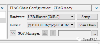
As shown, the SOF Manager is a small download manager; readers can also complete the download using a general download manager. However, all download activities must be executed after the configuration is complete (synthesis successful and downloaded).

② Signal Interface – Configure Capture Clock, Storage, Trigger: Once JTAG is ready, we can start executing signal-related configurations. As shown in Figure 3.6, the default signal interface looks like this, where:
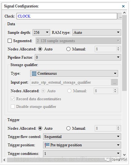
- Clock is the capture clock
- Sample depth is the storage/capture depth
- RAM Type is the storage resource
- Storage Qualifier – type is the storage method
First, let’s set the capture clock, so click the < … > next to the Clock option, which will pop up the node interface.
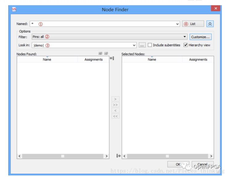
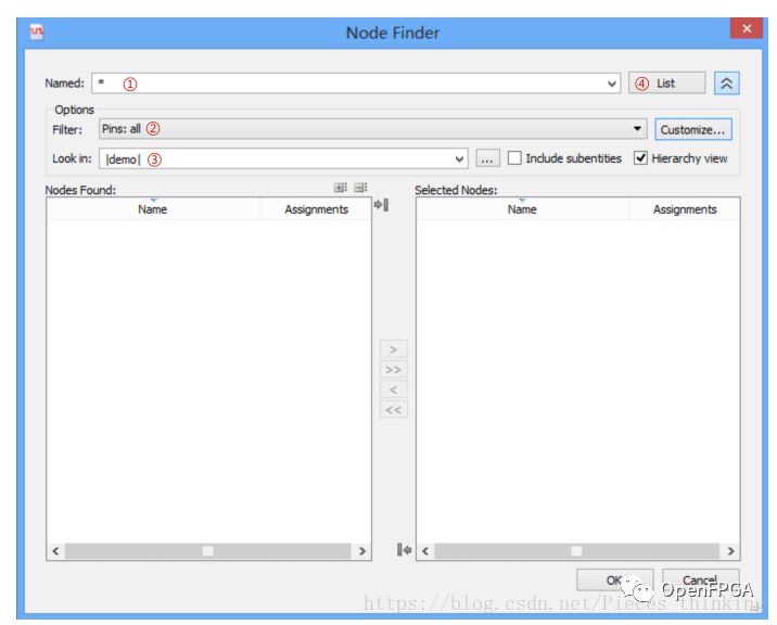
The figure shows the node interface; this is quite similar to Time Quest: (1) Please keep Named:* unchanged, (2) Set Filter to <Pins: all>, (3) Ensure Look in points to the top-level module, (4) Then click the > List on the upper right.
As shown in the figure, this is the process of adding nodes (capture clock): (1) Click to list all demo module related ports. (2) Among many ports, the node CLOCK will become the capture clock, then click it. (3) Click > to add this node to the right. (4) Click < OK > to apply the settings.
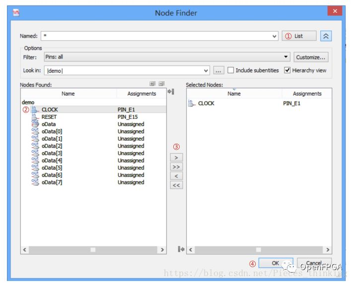
As shown in the figure, once the capture clock is set, the text box next to Clock will display the word CLOCK.

As shown in the figure, the general settings for storage-related configurations are usually as follows: (1) Sample depth is set according to preference, here it is 256. (2) RAM type storage resources, if set to Auto, it is very convenient; otherwise, it is M4K/M9K or Logic. (3) Storage qualifier – type, select Continuous for continuity.
Readers may not believe that as much as 80% of debugging work is done according to such settings and configurations.
As shown in Figure 3.11, the general settings for trigger-related configurations are usually as follows:
- Trigger flow control, choose Sequential for sequence.
- Trigger position, select Pre-trigger position.
- Trigger conditions, choose one for the number of trigger conditions. Similarly, readers may also not believe that as much as 80% of debugging work is done according to such trigger configurations. So far, the configuration work of the signal interface has come to an end.
③ Configuration Interface – Add Capture Objects: As shown in Figure 3.12, the configuration interface is where nodes (capture objects) are added. By default, it is empty, and we must add objects ourselves. (1) Right-click to bring up the menu, (2) Click
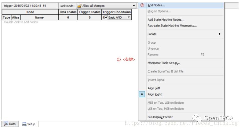 After completing the above two steps, the node interface will pop up.
As shown in the figure, the same node interface appears again: (1) Please keep Named:* unchanged, (2) Set Filter to <Pins: all>, (3) Set Look in to the top-level module, (4) Click to list all related ports of the demo module.
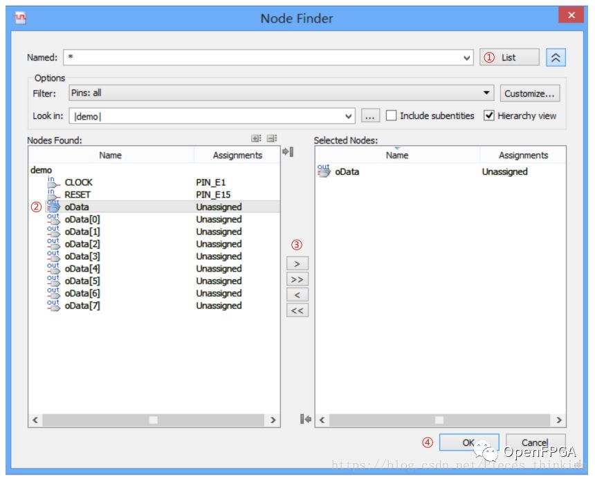
As shown in the figure, suppose oData is the capture object: (1) Click to list all ports related to the top-level demo module, (2) Select oData, (3) Click > to add the node to the right, (4) Click to apply the configuration. As shown in the figure, if everything is correct, the node (capture object) oData will appear in the configuration interface. After that, we can start configuring the trigger events.
 ④ Trigger Events:
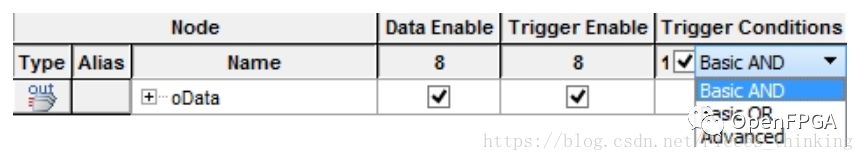
As shown in the figure, the author has previously mentioned that trigger events can be singular or plural, where Basic AND and Basic OR are used to express the relationship of multiple trigger events. We use the same example for explanation…
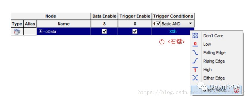
To get back to the point, the author has also mentioned that SignalTap has preset trigger events and advanced trigger events; the latter must set the trigger event to Advance. Conversely, preset trigger events can: (1) Right-click on the trigger event table box and (2) Select
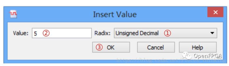
As shown in the figure, this is the situation after configuring the numerical trigger event: (1) Choose format, here it is <Unsigned Decimal>, (2) Input value, here it is 5, (3) Click to apply the configuration.
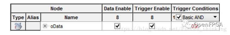
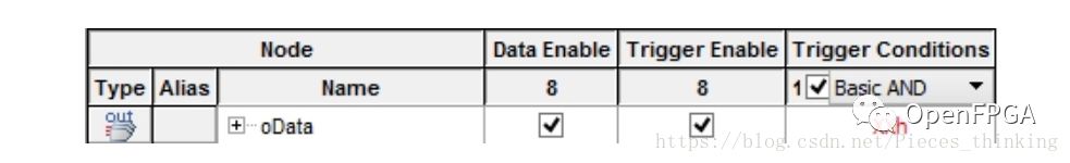
The above figure shows the situation after the trigger event configuration is completed, where oData is 5 for execution collection. So far, the configuration work is nearly complete; the remaining steps can be synthesized together and downloaded to the device. During this process, the system may require saving all configurations, such as stp1.stp, etc.; readers can save them anywhere.
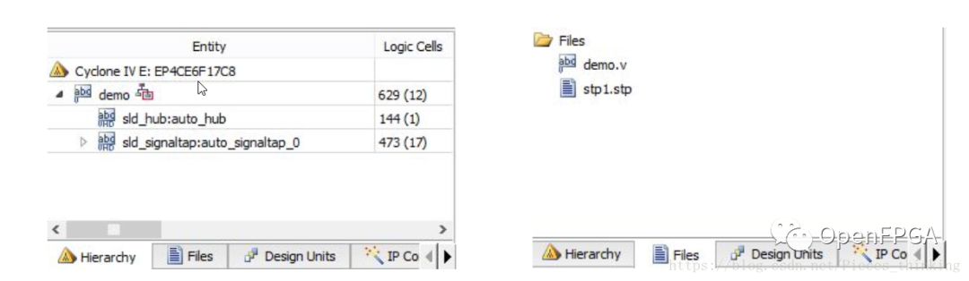
If everything is correct, the results of the three-level relationship and file relationship of the experiment are shown in the above figure, where sld_×× is the instantiation of the SignalTap module; readers can also consider it as a debugging module (environment).
⑤ Acquisition Interface: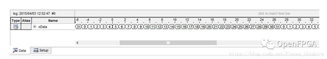
As shown in Figure 3.22, after the program is downloaded, if the environment creation fails, it will display in red (left figure). Conversely, if the environment creation is successful, it will print the words Ready to acquire. Generally, there are several reasons for debugging environment creation failure:
-
JTAG not ready
-
Program download failed
-
Synthesis result expired
-
Device not powered on
After eliminating the above four reasons, the debugging work will be in a ready state.
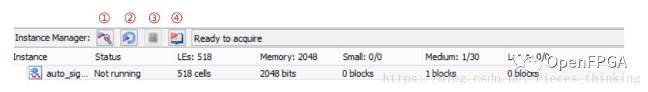
As shown in Figure 3.23, the acquisition interface mainly has four options to control the entire acquisition process: (1) Run Analysis manually executes the trigger event to induce acquisition, stopping automatically when reaching the acquisition count. (2) Auto Analysis automatically executes, ignoring trigger events and acquisition counts, capturing everything. (3) Stop, halts execution and acquisition. (4) Read Data, reads data, retrieving the contents of the buffer space. Generally, if the trigger event configuration is correct, we just need to press manual execution, and the trigger event will induce acquisition. When the acquisition reaches a certain count (based on storage depth), the acquisition process will end. Readers are not mistaken; the acquisition interface only has four options, among which manual execution is the most useful because the other options only come into play when acquisition fails (trigger events not met), which is quite ironic. For example, stop execution either forcibly stops an uncontrolled acquisition scene or is used in conjunction with auto execution. Conversely, reading data also forcibly retrieves data from the device (buffer space) in uncontrolled acquisition situations. Alright, let’s click manual execution and quietly collect results.

According to the demo module, we know it counts repeatedly from 0 to 31. As shown in Figure 3.24, T0 indicates the moment when the trigger event is met, which is also the start of the acquisition process, where the future value of 5 is the condition for the trigger event to be met… Simple debugging work concludes here.
3 (Supplement) Standard Debugging Process of Signal Tap As shown in Figure 3.25, although this is the officially designated standard process, the author still suggests just taking a look and not taking it too seriously. Believing in “standards” can easily lead to mistakes. One noteworthy point in Figure 3.25 is that when the trigger event fails, if one wanders along the process, it will require manual stopping of the analysis. If SignalTap displays results, then analyze; otherwise, forcefully read results from the device.
Finally, the author has also drawn a flowchart of the configuration process for Experiment Three, as shown in Figure 3.26; readers can look at it themselves.4 (Supplement) Adding Nodes
The author believes that many first-time learners will be intimidated by the node filtering options. As shown in Figure 3.27, the official has prepared many options for us, which can feel somewhat counterproductive. The filtering options can generally be divided into two categories to narrow down the scope. One is the Pin port type, and the other is the Reg register type. The options I like are only Pins: all and Register: pre-synthesis.