
Insights on Small FPGA Development

Insights on Small FPGA Development

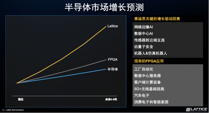
Lattice recently cited data from IHS at its new product launch event, indicating that the market growth rate for FPGA chips will outpace the overall semiconductor market over the next 4-6 years. While different research institutions provide varying estimates for the FPGA market size, this is indeed a consensus.
Typically, these reports mention potential drivers in sectors such as automotive ADAS, IoT, AI, and communications. Lattice lists existing FPGA applications including factory automation, data center servers, client computing devices, 5G+ wireless infrastructure, and automotive electronics.
From Lattice’s perspective, over the next 4-6 years, as a member of the FPGA market—and the largest supplier of FPGA shipments globally (and the largest supplier of small FPGAs)—the company’s growth rate is expected to exceed the average growth rate of the FPGA market.
Insights on Small FPGA Development
Lattice’s Senior Director of Applications Engineering for the Asia-Pacific region, Xie Zhengfan, mentioned that key growth drivers identified by Lattice include edge AI, data center AI, sensor-to-cloud interconnectivity, network security, and robotics.
An examination of the company’s financial reports over the past few years reveals that their revenue for fiscal year 2021 was approximately $515 million, $660 million in 2022, and $737 million in 2023. The 2023 report noted that product portfolio expansion was a significant factor in revenue growth, including the introduction of the Avant series mid-range FPGA two years ago, which expanded the market for previously available small FPGAs like Nexus; and continuous efforts to introduce new versions and application-specific solution stacks.
Thus, we believe that Lattice’s confidence in claiming that its business growth over the next 4-6 years will exceed the market average is crucially tied to the expansion of the market coverage of FPGA products themselves, as well as the introduction of solutions targeted at different applications.
At the recent Lattice Developer Conference, Lattice announced new products and corresponding software support: including the small FPGA Lattice Nexus 2 platform and the corresponding Certus-N2 series products; while the mid-range FPGA-oriented Avant platform also added Avant 30 and Avant 50 options. This can be regarded as product and market expansion.
New Nexus 2 Platform: Key Upgrades Include…
Lattice launched the Nexus platform at the end of 2019, focusing on “small FPGAs.” Lattice defines “small FPGA” as those with a logic density of less than 200K SLC. Over the years, this has remained Lattice’s primary domain. Currently, there are eight products under the Nexus platform, targeting different markets.
During the media event, Xie Zhengfan emphasized that Lattice’s chip products highlight five key characteristics: smallest size, lowest power consumption, context-aware edge AI, strongest security, and ease of use. These features are most vividly represented in Lattice’s Nexus platform. Readers familiar with Nexus platform FPGA chips should know that this series of chips has significant advantages in power consumption, performance, size, and security compared to competing products.
In the first half of this year, Lattice initiated a project called double Nexus, aimed at doubling the number of products in this series: offering different logic densities and packaging options. This decision was reportedly made after conducting customer surveys to understand demand. The new product options are expected to be launched in the market next year. This itself represents an expansion of products based on existing resources.
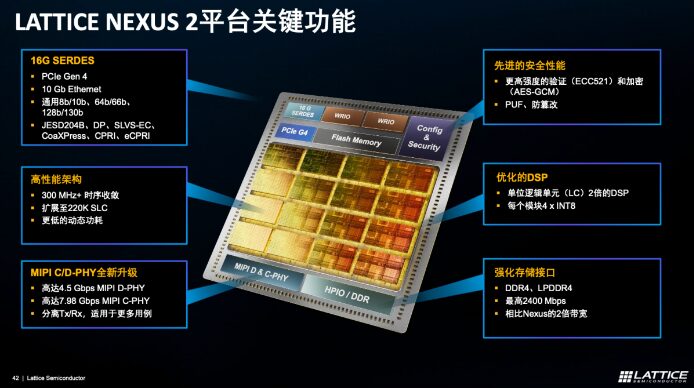
The newly released Nexus 2 platform is expected to enhance the aforementioned key points and is referred to by Lattice as the “next-generation small FPGA platform.” The three major improvements emphasized by Lattice remain “advanced interconnects,” “optimized power consumption and performance,” and “leading security performance.”
Insights on Small FPGA Development
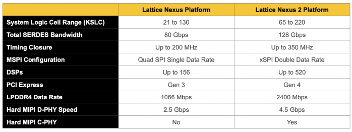
In terms of interconnects, the Nexus 2 platform supports high-speed MIPI D & C-PHY, with speeds up to 7.98Gbps; multi-protocol 16G SERDES, equipped with PCIe Gen 4 controllers; LPDDR4 interface supporting a maximum rate of 2.4Gbps (1033MT/s→2400MT/s).
The new platform has doubled the key performance metrics for interconnects compared to the previous Nexus, including doubled flash interface speeds and LPDDR4 rates. Therefore, it achieves faster transmission rate support based on offering more diverse interfaces.
Insights on Small FPGA Development
Power consumption and performance have always been Lattice’s strengths. Xie Zhengfan mentioned that the Nexus 2 platform “is optimized for small FPGAs in architecture and functionality, enhancing programmable speed while maintaining low power consumption advantages,” with frequencies increased to 350MHz. Additionally, the unit logic DSP has doubled, and the INT8 computation efficiency is also higher—thus it can better adapt to AI applications.
Regarding security, Nexus 2 emphasizes security algorithm updates to “address potential threats in the post-quantum era”—which likely refers to implementing certain industry-suggested quantum computing attack-resistant solutions in FPGAs, and relying on FPGA programmability to adjust deployed algorithms; integrated flash, fast boot, and “FPGA design and user data transmission security” also reflect Nexus 2’s security considerations.
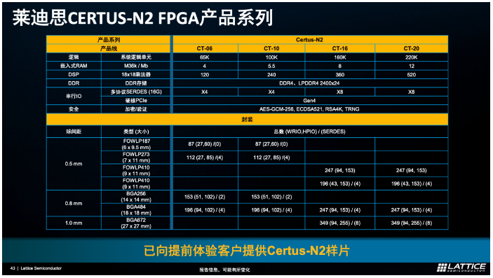
At the product level, the Nexus 2 platform will also have three product series: the general-purpose FPGA Certus, video interconnect CrossLink, and the control & security-focused Mach.
Insights on Small FPGA Development
This time, the Certus-N2 series was released, which is a general-purpose FPGA, with specific products and specifications as shown in the above image. Xie Zhengfan emphasized that Certus-N2 “can meet potential customer needs in system scalability and security bridging.”
Comparison of Nexus 2 with Two Competing Products
Performance, power consumption, and size advantages have always been Lattice’s traditional strengths, and Nexus 2 is no exception. This time, the comparison was made with Altera Cyclone 10GX 220 and AMD Artix UltraScale+ AU20P, comparing with the newly released Certus-N2 CT20.
In fact, based on Lattice’s ecological niche differences with the first two competitors, the competing products indeed have no advantage in the small FPGA field where Lattice excels. Therefore, in addition to presenting the comparison results, we finally have the opportunity to gain a deeper understanding of the reasons behind Lattice’s advantages in small FPGAs based on the publicly available Nexus 2 white paper.
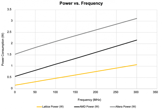
First, we compare power consumption. From the perspective of power consumption, Certus-N2 consumes one-third of its competitors.
Insights on Small FPGA Development
In this comparison, all three FPGA applications share the same RTL design; the RTL design occupies similar resources, about 107k SLC (61k LUT/122k registers). Across the full frequency range of 0-300MHz, Nexus 2 demonstrated power consumption advantages, including lower static and dynamic power consumption.
Nexus 2 does not continue to use FD-SOI technology like Nexus, but instead is based on 16nm FinFET technology. Although we know that FD-SOI has low power consumption advantages, the 16nm process shrink (compared to 28FDSOI) should theoretically achieve lower power consumption. The white paper also emphasizes the performance and power consumption value of LUT4 for small FPGAs from a design perspective.
In terms of security comparison, in addition to modern essential options such as encryption agility, quantum-safe encryption, and trusted roots, Lattice compared its Certus-N2 with competitors in configuration time. This is because chip loading speed is closely related to system security—”If our chip serves as a trusted root, the chip needs to power on and load quickly; otherwise, it will affect the security chain,” Xie Zhengfan noted.
For instance, to ensure industrial production safety, systems must have instant fault recovery capabilities, which relates to boot speed—such as in the case of intelligent sensor failures, which must be restored to work as quickly as possible.
Insights on Small FPGA Development
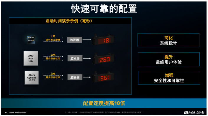
The above image compares the external flash configuration speed, with specific time values from INIT effective (assertion) to DONE signal pin effective time. Test results show that Certus-N2 is 15-20 times faster than the other two competitors.
The white paper lists factors affecting FPGA startup time, including not only the speed of the flash itself but also clock frequency, interface type, and configuration data size. Certus-N2’s flash clock frequency is the highest among the three (160MHz); in terms of interface type, Certus-N2 supports DDR xSPI flash interfaces, and at the same clock speed, the bandwidth is four times that of the QSPI used by competitors;
Insights on Small FPGA Development
Additionally, the LUT4 used in Nexus 2 has better area efficiency, while the larger structures of competing products result in more configuration data; hence, “the combination of smaller bitstreams and faster configuration interfaces provides significant advantages in startup time”—as shown in the above image.
Combining the above two points of fast configuration speed and low power consumption, for example, in system-level performance for applications like network edge sensor monitoring, Certus-N2’s power consumption is only one-tenth that of competitors based on dynamic power cycling between standby and operational states. Especially since Artix US+ and Cyclone 10GX have startup speeds that are more than ten times slower, the work and standby cycle switching within a unit time is mostly consumed in startup, making power saving impossible.
In addition, there are three other comparisons worth mentioning: (1) MIPI rate—As mentioned earlier, Nexus 2 has increased the MIPI rate to 7.98Gbps, making it three times that of competitors; (2) Chip packaging size—Certus-N2 achieves 11x9mm², while the packaging area of the two competing products is 3.7 times and 5.3 times larger, which should be largely related to process and structural choices;
Insights on Small FPGA Development
(3) TCO total cost of ownership: Just because of the configuration bitstream size, the selected flash specifications for Nexus 2 already have advantages. Coupled with the previously mentioned advantages of Certus-N2 in power consumption and size, savings in PCB and heat sink, and simpler power supply design lead to lower system BOM and development costs. Furthermore, in terms of maintenance costs, security and reliability designs significantly reduce these costs.
Readers interested in the Nexus 2 platform are encouraged to check out this white paper.
Avant Mid-Range FPGA Series Also Expands
In addition to the new Nexus 2 platform, Lattice also introduced new Avant 30 and Avant 50 products for the mid-range FPGA series at this developer conference, equipped with 300K and 500K logic units respectively. When the Avant series was first released, we elaborated on its significant value in expanding Lattice’s FPGA product line.
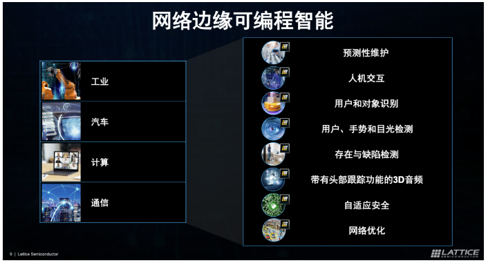
The Avant platform includes low-power FPGAs optimized for edge networks—Avant-E series; general-purpose FPGAs—Avant-G series; and FPGAs focused on interconnects—Avant-X. The newly updated Avant 30 and Avant 50 target all three series. Typical applications include “sensor fusion and AI processing” at edge locations, such as predictive maintenance, human-machine interaction, object recognition, gesture detection, presence and defect detection, etc.
“Combined with previously released 700K capacity products, the new products expand the mid-range FPGA capacity choices, providing new options for advanced interconnect and edge network applications,” Xie Zhengfan stated, noting that samples of Avant 30 and Avant 50 have already been provided to customers.
In our view, both the newly released Nexus 2 platform and the new Avant 30 and 50 with different logic resource options aim to precisely cover more potential applications and customers, with the goal of expanding market value to exceed the average development level of the semiconductor and FPGA markets in the next 4-6 years.
Insights on Small FPGA Development
As mentioned at the beginning, this market expansion goal cannot be achieved solely at the FPGA hardware level; it also requires supporting software tools and specific upper-level solutions—after all, chip companies generally produce chips while also focusing on terminal applications.
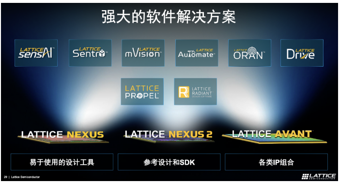
In addition to Lattice’s FPGA design development tools Propel and Radiant, which already support the newly released FPGA products, upper-level support targeting edge AI, security, vision, industrial, ORAN, automotive, and other sub-fields will naturally not be absent.
During the developer conference, new versions were released for Automate targeting factory automation, Drive for automotive, mVision for embedded vision, and sensAI for low-power edge AI.
Edge AI Holds Great Potential, Continued Optimism for Industrial and Automotive Markets
“Whether in data centers, industrial, automotive, client, or communications markets, leading global OEMs/ODMs are adopting our product solutions. Some are using their self-developed algorithms for FPGA design, while others are using our soft IP to accelerate product development speed.” It is said that Lattice’s partner ecosystem has expanded sixfold compared to 2018, as evidenced by the growing scale of the developer conference each year.
Lattice’s main business segments include “Communications and Computing,” “Industrial and Automotive,” and “Consumer.” In the current environment, where growth is slowing in the “Communications” market, seeking “new profit growth points” in the “Computing” market, and with uncertainties still existing in the “Consumer” market, Lattice sees market drivers mainly concentrated in three areas: the “intelligence” of edge network AI, the “interconnectivity” of sensors to the cloud, and the “security” of network resilience. All previously mentioned applications should be extensions of these three directions.
The importance of edge network AI was repeatedly emphasized during the media event. For AI inference at the edge, “in many cases, the data collected by sensors cannot be directly input into AI networks and requires pre-processing. This part of the work often relies on FPGAs.” “Integrating data pre-processing and AI inference into the same chip can achieve a single-chip edge AI solution.”
Moreover, with the programmability of FPGAs, for already deployed neural network algorithms, “optimizations can still be made during the future development phase,” whether for performance enhancement or functional expansion. This is the market opportunity Lattice sees in edge network AI and “programmable intelligence” at the network edge.
This opportunity, when targeting different vertical fields, has functional demands for predictive maintenance, human-machine interaction, object detection, gesture detection, etc. For example, specifically in automotive and industrial areas, “the DMS (Driver Monitoring System) in vehicles is an important application of AI in cars; predictive maintenance in industrial settings, as well as agricultural product classification, etc.”
Insights on Small FPGA Development
In fiscal year 2023, Lattice’s “Industrial and Automotive” business accounted for nearly 60% of its annual revenue. Therefore, Xie Zhengfan also mentioned that the order volume from domestic industrial customers in China has seen significant growth last year and this year—constituting the “largest driver” and “baseline” for Lattice’s revenue growth.
Automotive is also a field with a significant increase in customer numbers—”Previously, we provided about 2-3 new automotive solutions each year; however, in 2024, we expect to launch 5-6 different application solutions for automotive applications.” This includes solutions for DMS (Driver Monitoring System), OSD, head-up display, and other smart cockpit areas. Xie Zhengfan stated, “We remain very optimistic about the automotive market for next year.” “In the long term, the automotive market also holds the greatest potential.”
By relying on edge network AI as a key support, Lattice aims to continuously expand its automotive and industrial markets; while also continuously expanding its Nexus and Avant platform products to improve upper-level applications and solutions for customers. This generally outlines Lattice’s current market attitude and development thinking.

Insights on Small FPGA Development

Recommended Hot Articles
    • German Imported WiFi Signal Booster, After Opening… This Circuit is Amazing

    • I Took a Walk Around Huaqiangbei and Found Some New Gadgets…

    • From CoWoS to CoPoS, Chips Transition from Round to Square

    • 65 Chinese Scholars Selected as IEEE Fellows in 2025

    • CT Inspected Data Cables, Maliciously Embedded Chips!

Leave a Comment