Welcome FPGA engineers to join the official WeChat technical group.
Clickthe blue textto follow us at FPGA Home – the best and largest pure FPGA engineer community in China

Basic Concepts of Verilog Syntax
1. Verilog HDL
Verilog HDL is a language used for digital system design. The circuit design described by Verilog HDL is called a Verilog HDL model or module. Verilog HDL is both a behavioral description language and a structural description language. This means that modules can be created in Verilog to model circuit functionality or to describe the interconnections of components or larger parts. If written according to certain rules, behavioral modules can be automatically converted into gate-level interconnection modules by tools. Verilog models can be different levels of abstraction of the actual circuit. There are five common levels of abstraction and their corresponding model types:
1.1. System Level: Models the external performance of design modules using advanced structures provided by the language.
1.2. Algorithm Level: Models the algorithm operation using advanced structures provided by the language.
1.3. RTL Level: Describes the flow of data between registers and how to process and control this data flow.
1.4. Gate Level: Describes the logic gates and the connections between them.
1.5. Switch Level: Describes the transistors and storage nodes in devices and their connections.
2. Verilog HDL Modules
A complete Verilog HDL model of a complex circuit system consists of several Verilog HDL modules, each of which can be composed of several sub-modules. Some modules need to be synthesized into specific circuits, while others only interact with existing circuits designed by users or stimulus sources. This functionality provided by the Verilog HDL language structure allows for a clear hierarchical structure between modules to describe extremely complex large designs and to strictly verify the logic circuits of the designs made.
Verilog HDL behavioral description language, as a structured and procedural language, has a syntax structure that is very suitable for algorithm-level and RTL-level model design. This behavioral description language has the following functions:
(1) Can describe sequential or parallel execution program structures.
(2) Clearly controls the start time of processes using delay expressions or event expressions.
(3) Triggers activation or stop behaviors in other processes through named events.
(4) Provides conditions, if-else, case, and loop program structures.
(5) Provides tasks (task) program structures that can have parameters and non-zero duration.
(6) Provides function structures (function) that can define new operators.
(7) Provides arithmetic operators, logical operators, and bitwise operators for constructing expressions.
As a high-level hardware description programming language, Verilog has many similarities in style with C language. Many statements such as: if statements, case statements, etc. are very similar to corresponding statements in C language. If readers have mastered the basics of C language programming, learning Verilog HDL is not difficult. We just need to focus on understanding certain special aspects of Verilog HDL statements and strengthen hands-on practice to master it well, allowing us to utilize its powerful features to design complex digital logic circuit systems.
2.1. Simple Verilog HDL Module
2.1.1 Verilog Syntax Introduction
Now we will introduce a simple Verilog HDL program to understand the characteristics of Verilog modules.
module test_project_top( //Module Name
input clk, // Clock Input
input resetn, // Reset
input[7:0] a, //Signal Input, Signal a width is 8 bit
input[7:0] b, //Signal Input, Signal b width is 8 bit
input en, // Signal is enabled, Signal en width is 1 bit
output reg [8:0] c, // Register type definition, Signal output c is 9 bit
output reg [15:0] d // Register type definition, Signal output d is 16 bit
);
/*……..*/ //………Indicates the comment part, comments are only for the convenience of programmers to understand the program, and do not affect compilation.
/*A .v file mainly consists of one or more module … endmodule blocks
Each module block includes: module name, input ports, output ports, and several sequential circuits, combinational circuits, etc.
*/
// Simple Sequential Circuit Composition
always@(posedge clk or negedge resetn)
begin
if(~resetn) // or if(!resetn) take resetn inverse
begin
d<=16’h0;
end
else
begin
if(en) // if en ==1 then d equals a*b+a/b; otherwise d<=0
d<=a*b+a/b; // + , – ,* ,/ add, subtract, multiply, divide
else
d<=0;
end
end
// Simple Combinational Circuit
always@(a or b) // As long as one of a or b changes, execute the statements in the always block
begin
if(en) // verilog syntax if … else …, in combinational circuits, one if corresponds to one else, cannot lack else to prevent generating latches
c<=a*b+a/b;
else
c<=0;
end
wire[8:0] sum; // Common variable definition types: wire – wire type, reg – register
assign sum =a+b; // Combinational circuit assignment, keyword assign
wire[15:0] multy;
assign multy = (en ) ? a*b :0;// If en ==1, then multy =a*b, otherwise multy =0;
wire e;
assign e =&a; // & bitwise and
wire f;
assign f =|b;// | bitwise or
wire [8:0] c_sum;
// Instantiate Module
my_add u_add_top( // my_add Module Name, u_add_top Instance Name
.clk(clk), //Port connection input
.resetn(resetn),//Port connection input
.a(a),//Port connection input
.b(b),//Port connection input
.c(c_sum)//Port connection output
);
endmodule
This small program describes a .v file that includes common verilog syntax, variable definition types including: wire, reg, etc., common operators are the same as in C language, easy to understand. In this example, there are two modules. Module test_project_top references the instance part u_add_top defined by module my_add. Module test_project_top is the top module, while module my_add is called a sub-module. In instance part u_add_top, the part with “.” indicates the ports of the referenced module, the names must be consistent with the port definitions of the referenced module my_add, and the parentheses indicate the lines connected in this module.
2.1.2, Verilog for Module Testing
Verilog can also be used to describe changing test signals. The module that describes the changes in test signals and the testing process is also called a Testbench or Testfixture, which can dynamically test the circuit modules introduced above (whether behavioral or structural). By observing whether the output signals of the tested module meet the requirements, we can debug and verify whether the design and structure of the logic system are correct, and discover and modify problems in a timely manner.
Now let’s look at a Verilog test module,
// Test stimulus generation
`timescale 1ns / 1ps
module test_project_top_tb; // Test file module name
// Signal test stimulus, input variable declaration
reg clk ;
reg reset;
reg [7:0] a;
reg [7:0] b;
reg en;
// Output variable declaration
wire[8:0] c;
wire [15:0] d;
// Signal variable initialization, keyword initial
initial
begin
clk =0;
reset =0;
a =0;
b =0;
en =0;
#1000; // After 1000 ns reset goes high
reset =1;
end
// Clock generation
always #5 clk =~clk; //Clock cycle 10ns, flip every 5ns
always @(posedge clk)
begin // {$random} is a system task that generates a random number
#1 a= {$random}%256; // Generate random bit signal streams a and b, %256 is modulo 256
#3 b = {$random}%256; // Generate random bit signal streams a and b with delays of 1 and 3 time units respectively
end
always #10000 en = !en; //Generate a selection signal change with a period of 10000 time units
// Instantiate the tested module
test_project_top u_top(
.clk(clk), // Clock Input
.resetn(reset), // Reset
.a(a), //Signal Input, Signal a width is 8 bit
.b(b), //Signal Input, Signal b width is 8 bit
.en(en), // Signal is enabled, Signal en width is 1 bit
.c(c), // Register type definition, Signal output c is 9 bit
.d(d) // Register type definition, Signal output d is 16 bit
);
endmodule
This test routine is a test of the small program in 2.1.1, belonging to RTL level functional simulation, mainly debugging whether the syntax and timing signals are consistent with the design. For beginners, this is the most basic skill that must be mastered.
 Figure 1 Simulation Timing Diagram
2.1.3 Summary:
From the above examples, we can see the following points:
(1) Verilog HDL programs are composed of modules. The content of each module is located between the module and endmodule statements, and each module implements a specific function.
(2) Modules can be hierarchically nested. Because of this, large digital circuit designs can be divided into different small modules to achieve specific functions.
(3) Each module can be synthesized, and through synthesis tools, their functional descriptions can be converted into the most basic logic unit descriptions, which can then be connected together by a top-level module through instance references to form a large logic system.
(4) Verilog modules can be divided into two types: one is to allow the module to ultimately generate circuit structures, and the other is only to test whether the designed circuit’s logical functions are correct.
(5) Each module must define port definitions and specify input and output ports, and then describe the function of the module.
(6) The writing format of Verilog HDL programs is free; one line can write several statements, and one statement can also be written in multiple lines.
(7) Except for the endmodule statement, each statement and data definition must end with a semicolon.
(8) Comments can be made on any part of the Verilog HDL program using /*…..*/ and //……. A good, valuable source program should add necessary comments to enhance the readability and maintainability of the program.
Chapter 3 Verilog Syntax Advancement
3. Structure of Modules, Data Types, Variables, and Basic Operators
3.1. Structure of Modules
The basic design unit of Verilog is the “module” (block). A module consists of two parts, one part describes the interface, and the other part describes the logical function, that is, defining how the input affects the output. Below is an example:
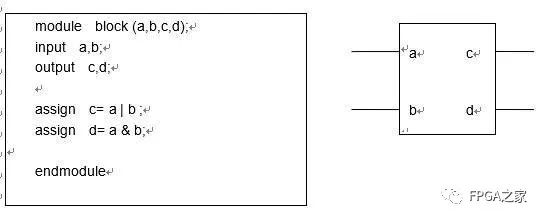 Figure 2 Module Schematic
Please look at the above example: The program module has a circuit diagram symbol next to it. In many ways, the program module and the circuit diagram symbol are consistent because the pins of the circuit diagram symbol are also the interface of the program module. The program module describes the logical function implemented by the circuit diagram symbol. This is all that is needed to design a simple Verilog program module. From the above example, it can be seen that the Verilog structure is located between the module and endmodule declaration statements, and each Verilog program includes four main parts: port definition, I/O description, internal signal declaration, and function definition.
3.1.1, Module Port Definition
The module port declares the input and output ports of the module. The format is as follows:
module ModuleName(port1, port2, port3, port4, ………);
…….
endmodule
The module ports represent the names of the module’s input and output ports, which are identifiers that link it to other modules. When a module is referenced, some signals need to be input into the referenced module, and some signals need to be taken out from the referenced module. There are two methods to connect the ports when referencing:
1) When referencing, connect strictly according to the order of the module definition ports without specifying the port names defined in the original module definition, as shown below:
ModuleName InstanceName( connecting port1 signal name, connecting port2 signal name, connecting port3 signal name,….,,, );
2) When referencing, use “.” to indicate the port names defined in the original module definition, as shown below:
ModuleName InstanceName(.port1Name( connecting signal1 name),.port2Name( connecting signal2 name),….,,, );
The advantage of this representation is that it can correspond to the port names with the ports of the referenced module without strictly following the port order, improving the readability and portability of the program.
3.1.2, Module Content
The content of the module includes I/O description, internal signal declaration, and function definition.
3.1.2.1, I/O description format is as follows:
Input Port: input [signal width – 1:0] port name1;
input [signal width – 1:0] port name2;
………;
input [signal width – 1:0] port namei; //(there are a total of i input ports)
Output Port: output [signal width – 1:0] port name1;
output [signal width – 1:0] port name2;
………;
output [signal width – 1:0] port namej; //(there are a total of j output ports)
Input/Output Port:
inout [signal width – 1:0] port name1;
inout [signal width – 1:0] port name2;
………;
inout [signal width – 1:0] port namek; //(there are a total of k bidirectional bus ports)
I/O description can also be written in the port declaration statement. The format is as follows:
module module_name(input port1,input port2,…
output port1,output port2… );
3.1.2.2, Internal Signal Declaration:
Declaration of wire and reg type variables used in the module and related to the port. For example:
reg [width – 1: 0] Rvariable1, Rvariable2 ….;
wire [width – 1: 0] Wvariable1, Wvariable2 ….;
………..
3.1.2.3, Function Definition:
The most important part of the module is the logical function definition part. There are three ways to generate logic in the module.
1) Use the “assign” declaration statement, such as: assign a = b & c;
2) Instantiate a module, such as: and u1( q, a, b );
3) Use the “always” block
For example: always @(posedge clk or posedge clr)
begin
if(clr) q <= 0;
else if(en) q <= d;
end
Using the “assign” statement is one of the most commonly used methods to describe combinational logic. The “always” block can be used to describe both combinational logic and sequential logic. The above example uses the “always” block to generate a D flip-flop with asynchronous clear. The “always” block can express logic using many methods, such as the example above using if…else statements to express logical relationships. When writing “always” blocks in a certain style, the source code can be automatically synthesized into combinational or sequential logic circuits represented by gate-level structures through synthesis tools.
3.1.3, Understanding Key Points:
If a Verilog module is to implement a certain function, it is necessary to clearly understand which occur simultaneously and which occur sequentially. The three items described above using the “assign” statement, instance components, and “always” blocks are executed simultaneously. That is, if these three items are written into a Verilog module file, their order does not affect the functional implementation. These three items are executed simultaneously, that is concurrently.
However, within the “always” module, the logic is executed in the specified order. The statements within the “always” block are called “sequential statements” because they are executed sequentially, so the “always” block is also called a “process block.” Note that two or more “always” statement blocks execute simultaneously, while the statements within the module execute sequentially. Look at the statements within the “always” block, and you will understand how the functionality is achieved. If…else… if must execute in order; otherwise, its functionality is meaningless. If the else statement is executed before the if statement, its functionality will not meet the requirements! To achieve the functionality described above, the statements within the “always” statement block will be executed in the order written.
In Verilog modules, all process blocks (such as: initial blocks, always blocks), continuous assignment statements, and instance reference statements are parallel. They represent a relationship that connects through variable names. The order of appearance of these three in the same module does not matter. Only continuous assignment statements (i.e., statements introduced by the keyword assign) and instance reference statements (i.e., statements introduced by the defined module name) can exist independently of process blocks in the functional definition part of the module. This is very different from C language. Many statements similar to C language can only appear in process blocks and cannot appear freely in the functional definition range of the module.
3.2, Data Types and Their Constants, Variables
There are a total of nineteen data types in Verilog HDL, which are used to represent data storage and transmission elements in digital circuit hardware. First, let’s introduce the four basic data types: reg type, wire type, integer type, and parameter type.
Other data types also include: large type, medium type, scalared type, time type, small type, tri type, trio type, tri1 type, triand type, trior type, trireg type, vectored type, wand type, wor type.
3.2.1, Constants
In the course of program execution, quantities whose values cannot be changed are called constants. Below is an introduction to the numbers used in Verilog HDL language and their representation methods.
3.2.1.1, Integers:
In Verilog HDL, integer constants have the following four base representations:
1) Binary integer (b or B)
2) Decimal integer (d or D)
3) Hexadecimal integer (h or H)
4) Octal integer (o or O)
3.2.1.2, x and z values:
In digital circuits, x represents an uncertain value, and z represents a high-impedance value. An x can be used to define the state of a four-bit binary number in hexadecimal, three bits in octal, or one bit in binary. The representation of z is similar to x. z can also be written as ?. It is recommended to use this notation when using case expressions to improve the readability of the program. See the example:
4’b10x0 // The binary number with a width of 4 has an uncertain value in the second bit from the low bit
4’b101z // The binary number with a width of 4 has a high-impedance value in the first bit from the low bit
12’dz // The decimal number with a width of 12 has a high-impedance value (first representation)
12’d? // The decimal number with a width of 12 has a high-impedance value (second representation)
8’h4x // The hexadecimal number with a width of 8 has an uncertain value in the low four bits
3.2.1.3, Negative Numbers:
A number can be defined as a negative number by simply adding a minus sign before the width expression; the minus sign must be placed at the very front of the number definition expression. Note that the minus sign cannot be placed between the width and the base, nor between the base and the actual number. As follows:
-8’d5 // This expression represents the complement of 5 (represented in eight-bit binary)
8’d-5 // Invalid format
3.2.2, Parameter (Parameter) Type
In Verilog HDL, parameters are used to define constants, that is, parameters define an identifier representing a constant, called symbolic constants, which improves the readability and maintainability of the program. Parameter type data is a constant type of data, and its description format is as follows:
parameter parameterName1=expression, parameterName2=expression, …, parameterNameN=expression;
parameter is the confirmation symbol for parameter type data, followed by a statement of assignment separated by commas. Each assignment statement on the right must be a constant expression. This means that the expression can only contain numbers or previously defined parameters. See below:
parameter msb=7; // Define parameter msb as constant 7
parameter e=25, f=29; // Define two constant parameters
parameter r=5.7; // Declare r as a real type parameter
parameter byte_size=8, byte_msb=byte_size-1; // Assign value using constant expression
parameter average_delay = (r+f)/2; // Assign value using constant expression
3.2.3, Variables
3.2.3.1, wire type
Wire type data is commonly used to represent combinational logic signals specified by the assign keyword. The input and output signal types in Verilog program modules are automatically defined as wire type by default. The format of wire type signals is very similar to that of reg type signals. Its format is as follows:
wire [n-1:0] DataName1, DataName2,…DataNamei;// There are a total of i buses, each bus has n lines
wire [n:1] DataName1, DataName2,…DataNamei;
wire is the confirmation identifier for wire type data, [n-1:0] and [n:1] represent the bit width of the data, that is, how many bits the data has. Finally, the names of the data follow. If multiple data are defined at once, the data names are separated by commas. The last statement of the declaration must end with a semicolon. As follows:
wire a; // Defined a one-bit wire type data
wire [7:0] b; // Defined an eight-bit wire type data
wire [4:1] c, d; // Defined two four-bit wire type data
3.2.3.2, reg type
Registers are abstractions of data storage units. The keyword for register data type is reg. The value stored in the register can be changed through assignment statements, which is equivalent to changing the value stored in a trigger. The default initial value of reg type data is uncertain value, x. Reg type only indicates that the defined signal will be used in the “always” block.
Reg type data is commonly used to represent specified signals used in “always” modules, often representing triggers. Typically, in a design, the logical relationship is expressed using behavioral description statements in the “always” block. Each signal assigned within the “always” block must be defined as reg type.
The format of reg type data is as follows:
reg [n-1:0] DataName1, DataName2,… DataNamei;
reg [n:1] DataName1, DataName2,… DataNamei;
reg is the confirmation identifier for reg type data, [n-1:0] and [n:1] represent the bit width of the data, that is, how many bits the data has. Finally, the names of the data follow. If multiple data are defined at once, the data names are separated by commas. The last statement of the declaration must end with a semicolon. As follows:
reg rega; // Defined a one-bit named rega reg type data
reg [3:0] regb; // Defined a four-bit named regb reg type data
reg [4:1] regc, regd; // Defined two four-bit named regc and regd reg type data
3.2.3.3, memory type
Verilog HDL models memory by establishing arrays of reg type variables, which can describe RAM type memory, ROM memory, and reg files. Each unit in the array is addressed through an array index. In Verilog language, there is no existence of multi-dimensional arrays. Memory type data is generated by extending the address range of reg type data. Its format is as follows:
reg [n-1:0] memoryName[m-1:0];
or reg [n-1:0] memoryName[m:1];
Here, reg[n-1:0] defines the size of each storage unit in the memory, i.e., each storage unit is an n-bit register. The memory name followed by [m-1:0] or [m:1] defines how many such registers are in the memory. The definition statement must end with a semicolon. Below is an example:
reg [7:0] mema[255:0];
This example defines a memory named mema, which has 256 eight-bit storage units. The address range of this memory is from 0 to 255. Note: The expression used for addressing memory must be a constant expression.
Additionally, within the same data type declaration statement, both memory type data and reg type data can be defined simultaneously. See the example below:
parameter wordsize=16, // Define two parameters
memsize=256;
reg [wordsize-1:0] mem[memsize-1:0], writereg, readreg;
Although the definition format of memory type data and reg type data is very similar, it is important to note their differences. For example, a memory group composed of n one-bit registers is different from an n-bit register. See the example below:
reg [n-1:0] rega; // An n-bit register
reg mema [n-1:0]; // A memory group composed of n one-bit registers
An n-bit register can be assigned a value in a single assignment statement, while a complete memory cannot. See the example below:
rega =0; // Legal assignment statement
mema =0; // Illegal assignment statement
If you want to perform read and write operations on the storage unit in memory, you must specify the address of that unit in memory. The following writing is correct.
mema[3]=0; // Assign the value of 0 to the third storage unit in memory.
The address index for addressing can be an expression, allowing operations on different units in memory. The value of the expression can depend on the values of other registers in the circuit. For example, a counter can be used to index the address of RAM.
3.3, Operators and Expressions
Verilog HDL language has a wide range of operators, which can be classified into the following categories based on their functions:
1) Arithmetic operators (+, −, ×, /, %)
2) Assignment operators (=, <=)
3) Relational operators (>, <, >=, <=)
4) Logical operators (&&, ||, !)
5) Conditional operators (?:)
6) Bitwise operators (~, |, ^, &, ^~)
7) Shift operators (<<, >>)
8) Concatenation operators ({ })
9) Others
In Verilog HDL language, the operators carry different operands, based on the number of operands the operators can be divided into three types:
1) Unary operator: can carry one operand, the operand is placed on the right side of the operator.
2) Binary operator: can carry two operands, the operands are placed on both sides of the operator.
3) Ternary operator: can carry three operands, these three operands are separated by the ternary operator.
clock = ~clock; // ~ is a unary negation operator, clock is the operand.
c = a | b; // is a binary bitwise OR operator, a and b are operands.
r = s ? t : u; // ?: is a ternary conditional operator, s, t, u are operands.
Below are some common operators introduced.
3.3.1, Basic Arithmetic Operators
In Verilog HDL language, arithmetic operators are also called binary operators and include the following:
1) + (Addition operator, or positive value operator, such as rega + regb, +3)
2) − (Subtraction operator, or negative value operator, such as rega – 3, -3)
3) × (Multiplication operator, such as rega * 3)
4) / (Division operator, such as 5 / 3)
5) % (Modulo operator, or remainder operator, requires that both sides of % be integer data. For example, 7 % 3 equals 1)
3.3.2, Bitwise Operators
Verilog HDL, as a hardware description language, is targeted at hardware circuits. In hardware circuits, signals have four state values: 1, 0, x, z. When signals are ANDed, ORed, or NOTed in circuits, this is reflected in Verilog HDL as corresponding bitwise operations on the operands.
3.3.2.1,