Source: Sensor Technology
Source: Reliability Technology Exchange
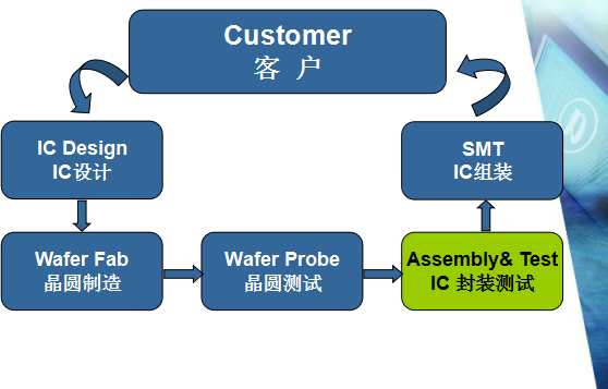
IC Package (the form of IC encapsulation) refers to the different shapes of the encapsulation formed by the chip (Die), various types of frameworks (L/F), and encapsulation materials (EMC).
There are many types of IC Packages, which can be classified according to the following standards:
Classified by encapsulation materials:
Metal encapsulation, ceramic encapsulation, plastic encapsulation
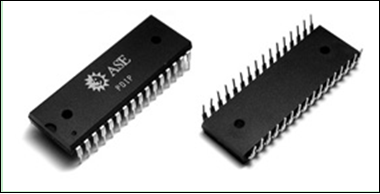
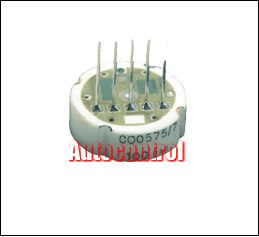
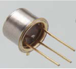
Metal encapsulation is mainly used in military or aerospace technology, with no commercial products;
Ceramic encapsulation is superior to metal encapsulation and is also used in military products, occupying a small commercial market;
Plastic encapsulation is used for consumer electronics due to its low cost, simple process, and high reliability, holding a vast majority of the market share;
Classified by connection method with PCB:
PTH encapsulation and SMT encapsulation
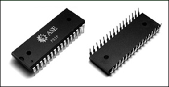
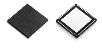
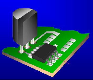
PTH – Pin Through Hole, through-hole type;
SMT – Surface Mount Technology, surface mount type.
Currently, most ICs on the market adopt the SMT type.
Classified by encapsulation shape:
SOT, SOIC, TSSOP, QFN, QFP, BGA, CSP, etc.;
Two key factors determining the encapsulation form:
Encapsulation efficiency. Chip area/encapsulation area should be as close to 1:1 as possible;
Number of pins. The more pins, the higher the level, but the difficulty of the process also increases accordingly;
Among them, CSP has achieved a chip area/encapsulation area of 1:1 due to the use of Flip Chip technology and bare chip encapsulation, making it the highest-level technology at present;
-
QFN – Quad Flat No-lead Package
-
SOIC – Small Outline IC
-
TSSOP – Thin Small Shrink Outline Package
-
QFP – Quad Flat Package
-
BGA – Ball Grid Array Package
-
CSP – Chip Scale Package
-
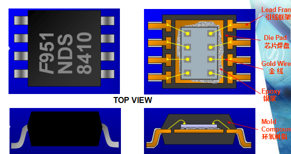
IC Package Structure (IC structure diagram)
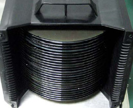
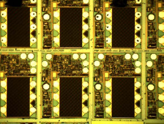
Raw Material in Assembly (Encapsulation Raw Materials)【Wafer】
【Lead Frame】
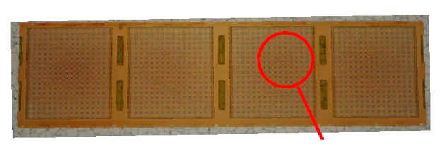
Provides circuit connection and Die fixation;
Main material is copper, which will be plated with silver, NiPdAu, and other materials;
The L/F process has two types: Etch and Stamp;
It is prone to oxidation and should be stored in a nitrogen cabinet with humidity below 40% RH;
Except for BGA and CSP, other Packages will use Lead Frame, while BGA uses Substrate;
【Gold Wire】
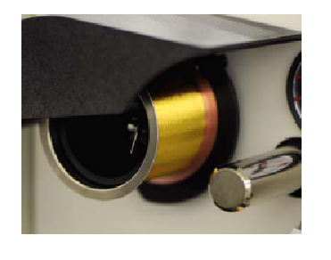
Realizes the electrical and physical connection between the chip and the external lead frame;
Gold wire uses 99.99% high purity gold;
Currently, for cost considerations, there are also processes using copper wire and aluminum wire. The advantages are cost reduction, but the process difficulty increases, leading to lower yield;
Wire diameter determines the current that can be conducted; 0.8mil, 1.0mil, 1.3mils, 1.5mils, and 2.0mils;
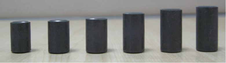
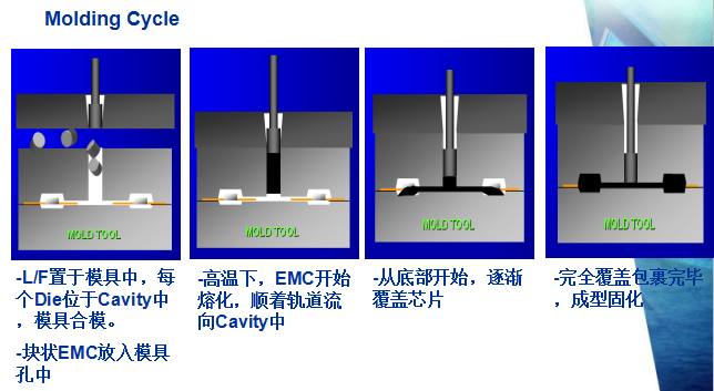
Mold Compound encapsulation material/epoxy resin mainly consists of: epoxy resin and various additives (curing agents, modifiers, release agents, colorants, flame retardants, etc.);
Main functions: to wrap the Die and Lead Frame in a molten state, providing physical and electrical protection, preventing external interference;
Storage conditions: stored at -5°; under normal temperature, it needs to acclimate for 24 hours;
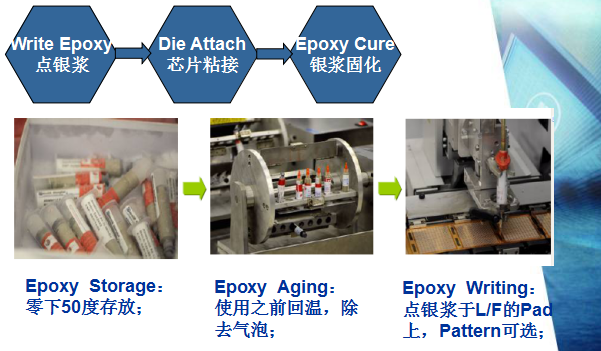
【Epoxy】silver paste
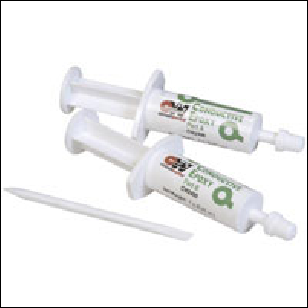
Consists of epoxy resin filled with metal powder (Ag); has three functions: fixes the Die on the Die Pad; dissipates heat, conducts electricity;
Stored below -50°, and needs to acclimate for 24 hours before use;
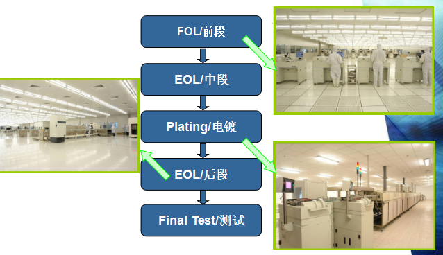
FOL– Front of Line
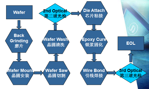
FOL– Back Grinding
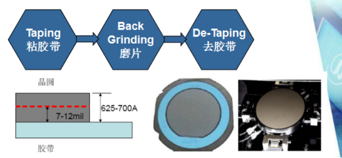
Back grinding of the Wafer coming out from the wafer factory to reduce the thickness of the wafer to reach the packaging requirements (8mils~10mils);
During grinding, tape should be applied to the front side (Active Area) to protect the circuit area while grinding the back. After grinding, remove the tape and measure the thickness;
FOL– Wafer Saw
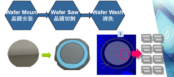
Paste the wafer on a blue film (Mylar) so that even if cut, it will not scatter;
Use Saw Blade to cut the entire Wafer into individual Dice for the subsequent Die Attach process;
Wafer Wash mainly cleans the dust generated during the Saw, cleaning the Wafer;
FOL– 2nd Optical Inspection
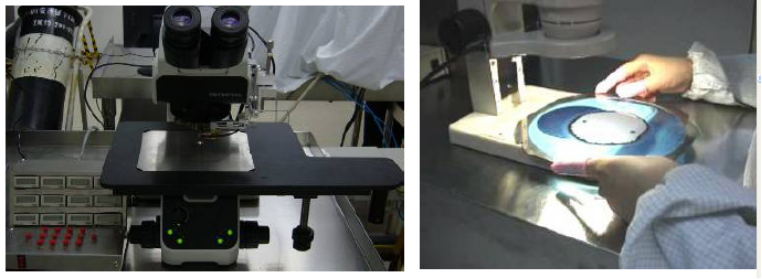
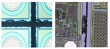
Mainly for the visual inspection of the Wafer after the Wafer Saw under a microscope, to check if there are any defects.
FOL– Die Attach
Chip pickup process:
1. Ejector Pin lifts the chip from below the wafer, making it easy to detach from the blue film;
2. Collect/Pick up head sucks the chip from above, completing the transport from the Wafer to the L/F;
3. Collect applies a certain force to bond the chip onto the Pad with silver paste on the L/F, with specific position control;
4. Bond Head Resolution: X-0.2um; Y-0.5um; Z-1.25um;
5. Bond Head Speed: 1.3m/s;
FOL– Epoxy Cure
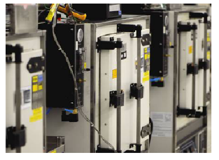
Silver paste curing:
175°C, 1 hour; N2 environment to prevent oxidation:
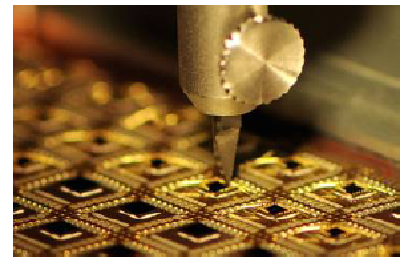
Die Attach quality inspection:
Die Shear (chip shear force)
FOL– Wire Bonding
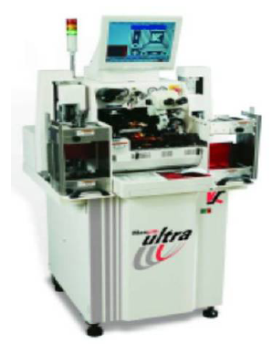
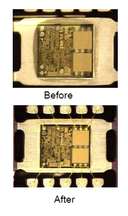
Using high purity gold wire (Au), copper wire (Cu), or aluminum wire (Al) to connect the Pad and Lead by welding. The Pad is the external connection point of the circuit on the chip, and the Lead is the connection point on the Lead Frame.
W/B is the most critical process in the packaging process.
FOL– 3rd Optical Inspection
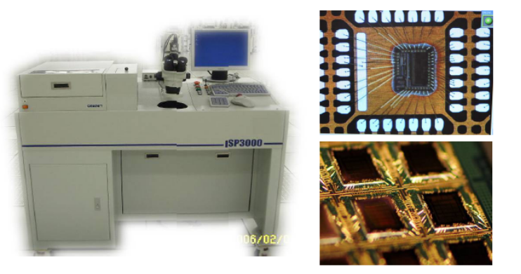
EOL– End of Line
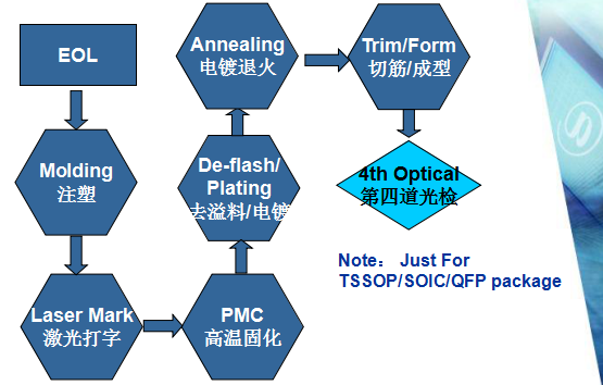
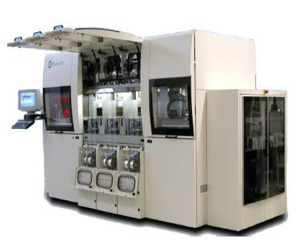
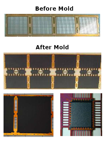
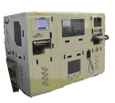
EOL– Molding
EOL– Laser Mark
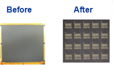
Laser engraving on the front or back of the product (Package). The content includes: product name, production date, production batch, etc.;
EOL– Post Mold Cure
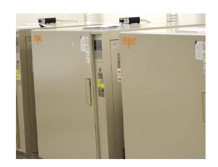
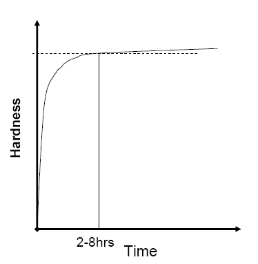
Used for curing the molding material after molding, protecting the internal structure of the IC, and eliminating internal stress. Cure Temp: 175+/-5°C; Cure Time: 8Hrs
EOL– De-flash
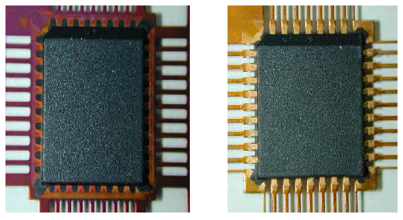
Purpose: The purpose of De-flash is to remove excess flash around the Leads after Molding; Method: weak acid soaking, high-pressure water washing;
EOL– Plating
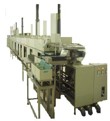
Using metal and chemical methods, a layer of coating is plated on the surface of the Leadframe to prevent external environmental influences (moisture and heat). This also makes it easier for components to be soldered onto the PCB and improves conductivity.
There are generally two types of plating:
Pb-Free: Lead-free plating, using >99.95% high purity tin (Tin), which is the currently widely adopted technology and meets RoHS requirements;
Tin-Lead: Tin-lead alloy. Tin accounts for 85%, Lead accounts for 15%, which is now basically eliminated due to non-compliance with RoHS;

EOL– Post Annealing Bake
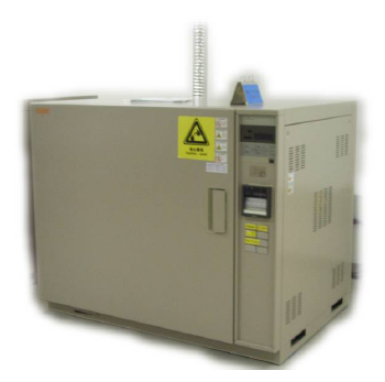
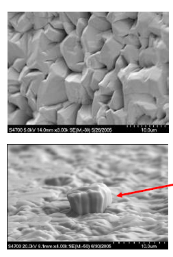
Purpose: To bake the lead-free plated product at high temperatures for a period to eliminate potential whisker growth issues in the plating layer; Conditions: 150+/-5°C; 2Hrs;
EOL– Trim&Form
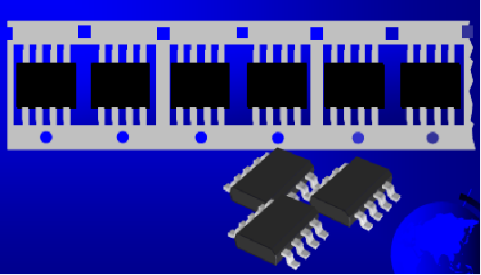
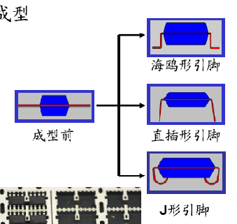
Trim: The process of cutting a strip of Lead Frame into individual Units (IC); Form: the process of shaping the pins of the trimmed IC product to meet the required shape for the process, and placing it into tubes or trays;
EOL– Final Visual Inspection
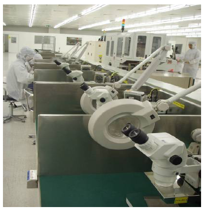
Under low magnification, inspect the appearance of the product. Mainly targeting defects that may occur during the EOL process: such as molding defects, plating defects, and trim/form defects.
Public account ID:imecas_wx