
Introduction: Spreading knowledge and broadening horizons. A technical repository. See the world with a unique perspective, interesting and informative.
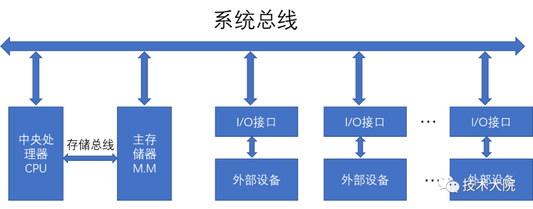
【Guide】 Engineers often use a set of lines, configured with appropriate interface circuits, to connect various components and peripheral devices, referred to as a bus, to simplify hardware circuit design and system structure. A bus is a common communication line for transmitting information between various functional components of a computer; it is a transmission line bundle made up of wires, classified according to the type of information transmitted by the computer. In simple terms, a bus is an internal structure, serving as a public channel for information transmission between the CPU, memory, and input/output devices. Today, we will discuss commonly used buses from a software perspective.
Classification of Buses
Divided by Function and Specification:
-
Data Bus: ISA, EISA, VESA, PCI
-
Address Bus
-
Specifically used to transmit addresses
-
Always unidirectional, the address can only be transmitted from the CPU to external memory or I/O ports
-
The number of bits in the address bus determines the size of the memory space that the CPU can directly address
-
Control Bus
-
Used to transmit control signals and timing signals
-
Some control signals are sent from the microprocessor to memory and I/O interface circuits
-
Others are feedback from other components to the CPU, such as interrupt request signals, reset signals, bus request signals, device ready signals, etc.
-
Expansion Bus
-
Local Bus
The data bus, address bus, and control bus are collectively referred to as the system bus, which is what is commonly meant by the term bus.
Divided by the Method of Data Transmission:
-
Serial Bus: Binary data is sent bit by bit through a single data line to the destination device
-
Parallel Bus: A parallel bus typically has more than two data lines
-
SPI
-
I2C
-
USB
-
RS232
Divided by Whether the Clock Signal is Independent:
-
Synchronous Bus: The clock signal is independent of the data; SPI and I2C are synchronous serial buses
-
Asynchronous Bus: The clock signal is extracted from the data; RS232 is an asynchronous serial bus
Generally, Buses in Microcomputers Include:
-
Internal Bus
-
The bus between various peripheral chips and the processor inside the microcomputer, used for interconnection at the chip level
-
System Bus
-
The bus between each plug-in board and the system board in the microcomputer, used for interconnection at the plug-in board level
-
External Bus
-
The bus between the microcomputer and external devices, where the microcomputer acts as a device to exchange information and data with other devices through this bus, used for interconnection at the device level
Buses Commonly Used in Automotive Networks:
-
LIN Bus
-
A low-cost serial communication network used to implement distributed electronic control systems in vehicles, serving as an auxiliary bus network
-
LIN bus can significantly reduce costs in scenarios where the bandwidth and multifunctionality of the CAN bus are not needed
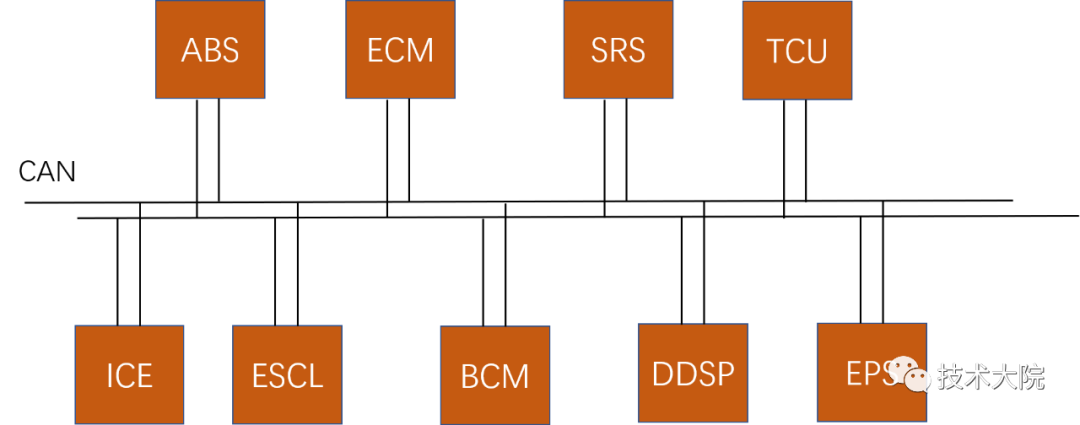
-
CAN Bus
-
Data transmission between control units and control plans
-
Supports UDS diagnostics, BT download testing, etc., from physical layer, data link layer, protocol layer, application layer, etc.
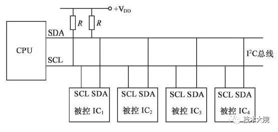
I2C Bus
I2C Bus: Developed by Philips, it is a two-wire serial bus that emerged in the 1980s for connecting microcontrollers and their peripheral devices.
Features:
-
I2C bus is simple and effective, occupying very little PCB (Printed Circuit Board) space
-
Fewer chip pins, lower design costs
-
I2C bus supports multi-mastering mode, where any device capable of sending and receiving can become a master device
-
The master can control data transmission and clock frequency, but only one master can exist at any given time
-
The two signals that make up the I2C bus are the data line SDA and the clock SCL
To avoid bus signal confusion, devices connected to the bus must have an open-drain output or collector-open output structure.
When the bus is idle, pull-up resistors keep both SDA and SCL lines high.
Timing:
The serial data line SDA interface circuit on I2C devices is bidirectional, with the output circuit used to send data onto the bus and the input circuit used to receive data from the bus. Similarly, the serial clock line SCL is also bidirectional.
-
The host controlling data transmission on the bus sends clock signals through the SCL output circuit and monitors the SCL level on the bus to determine when to send the next clock pulse
-
The slave device receiving commands from the host must send or receive signals on SDA according to the SCL signal on the bus; it can also send a low-level signal to the SCL line to extend the bus clock signal period
-
When SCL stabilizes at a high level, a change from high to low on SDA generates a start bit, while a change from low to high generates a stop bit, as shown in Figure 1
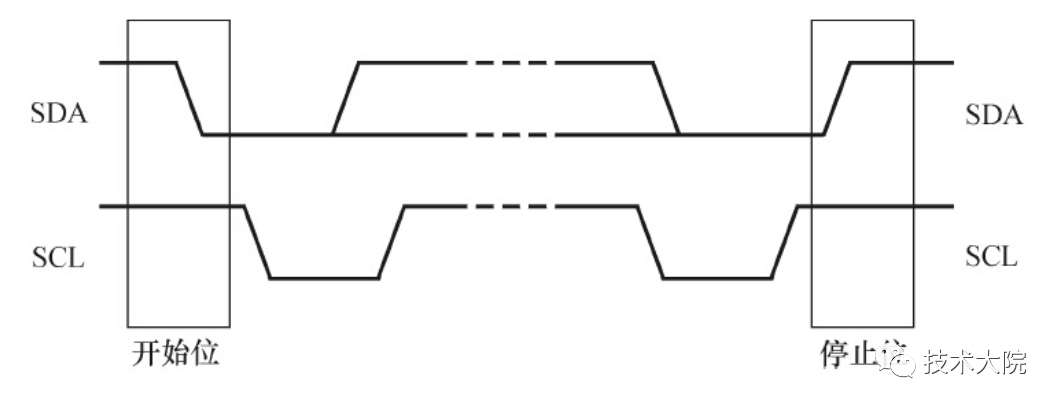
Start and stop bits are generated by the I2C master device
-
When selecting a slave device, if the slave device uses a 7-bit address, the master device must first send a 1-byte address information before initiating the transmission process, where the first 7 bits are the device address, and the last bit is the read/write flag
-
Then, each byte of data transmitted is also 1 byte, starting transmission from the MSB
-
After each byte is transmitted, the receiver should send an ACK bit before the 9th rising edge of SCL arrives.
-
The clock pulses on SCL are sent by the I2C master, and after the 8th clock cycle, the master should release SDA; the timing of the I2C bus is shown in Figure 2

Figure 2 Timing of I2C Bus
SPI Bus
SPI (Serial Peripheral Interface): A synchronous serial peripheral interface that allows the CPU to communicate with various peripheral devices in a serial manner to exchange information. Generally, the master SoC acts as the “master” of SPI, while peripherals act as the “slaves”.
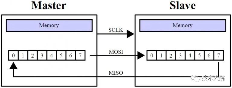
SPI interface generally uses 4 lines:
-
Serial Clock Line (SCLK)
-
Master Input/Slave Output Data Line (MISO)
-
Master Output/Slave Input Data Line (MOSI)
-
Low-level active Slave Select Line (SS)
-
In different literature, it is often referred to as nCS, CS, CSB, CSN, nSS, STE, SYNC, etc.
As shown in Figure 3, one master connects to three SPI peripherals:
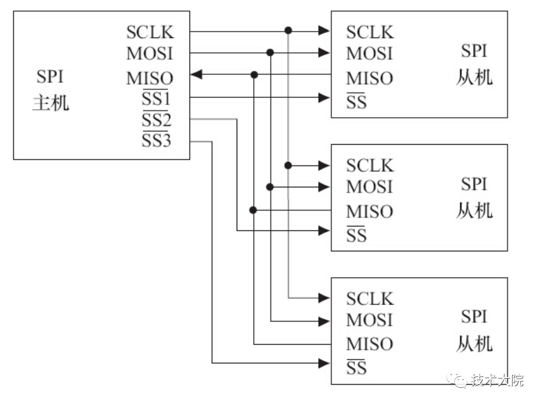
Figure 3 SPI Master-Slave Hardware Connection Diagram
Timing:
In SPI bus transmission, the SS signal is low-level active, and when we need to communicate with a peripheral, we need to pull the SS line of that peripheral low.
Additionally, it is particularly important to note the maximum clock frequency supported by the SPI slave device (which determines the frequency of SCK) and the CPHA and CPOL modes of the peripheral, which determine the offset between data and clock, the sampling timing, and whether the triggering edge is rising or falling.
Figure 4 Timing of SPI Bus
The SPI module configures its output serial synchronous clock polarity (CPOL) and phase (CPHA) according to the working requirements of the peripheral for data exchange:
-
CPOL=0, the idle state of the serial synchronous clock is low
-
Data is sampled on the first transition edge (rising or falling)
-
CPOL=1, the idle state of the serial synchronous clock is high
-
Data is sampled on the second transition edge (rising or falling)
USB Bus
USB (Universal Serial Bus): Proposed by manufacturers such as Intel and Microsoft in 1995 to solve the increasing variety of computer peripherals and the limited motherboard slots and ports.
Features:
-
Control Transfer: Reliable, time guaranteed
-
Bulk Transfer: Reliable, no time guarantee, e.g., USB flash drives
-
Interrupt Transfer: Reliable, real-time, e.g., USB mouse
-
Real-Time Transfer: Unreliable, real-time, e.g., USB camera
-
The USB communication process is always a master-slave structure, where the USB host initiates communication requests, and the device responds with data
-
USB devices do not have the ability to actively communicate with the host
-
The object of USB transmission is endpoints, each endpoint has a transmission type and direction
-
Endpoint 0 is used for control transfer, capable of both output and input
-
Except for endpoint 0, all other endpoints support data transmission in only one direction
-
Input (IN) and Output (OUT) are both stated from the perspective of the USB host; for example, the data from a mouse goes to the PC, and the corresponding endpoint is referred to as the “input endpoint”
USB Hardware Structure
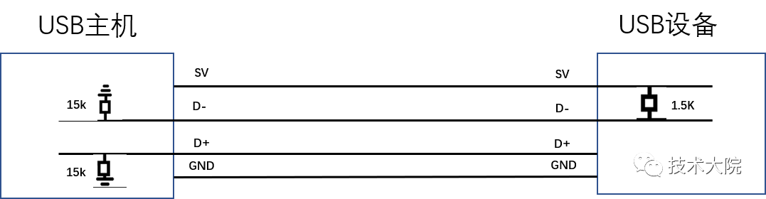
Figure 5 USB Hardware Structure
As shown in Figure 5:
-
The hub (USB Root Hub) has two data lines (D+ and D-), both connected with 15K pull-down resistors
-
When no device is connected, the voltage of the hub data lines D+ and D- is low
-
When a device is connected, the data line of the device is connected to a 1.5K pull-up resistor, causing one data line to be pulled high
-
The hub detects the connection of a device based on the high state of the data line and judges whether the connected device is a full-speed USB device (D+ is high) or a low-speed USB device (D- is high)
USB Connection Identification Process:
-
Hardware insertion, a level change on D+ or D- notifies the host
-
The host interacts with the USB device through endpoint address 0, assigning an address to the USB slave device
-
Obtaining information from the slave device through endpoint 0
-
Installing the corresponding device driver, providing functions to read and write to the device
USB Operating Modes:
-
Low Speed: Rate of 1.5Mbit/s, supports devices with low data throughput and real-time requirements, such as mice
-
High Speed:
-
In USB2.0, a high-speed mode is added, achieving a data transfer rate of 480Mbit/s, half-duplex, meeting the needs of higher-speed peripherals
-
Full Speed: Rate of 12Mbit/s, can connect peripherals with higher speeds
-
Super Speed USB:
-
USB 3.0 (also considered Super Speed USB) has a maximum transmission bandwidth of up to 5.0Gbit/s (i.e., 640MB/s), full-duplex
Ethernet Port
Ethernet Interface: The Ethernet MAC is defined by the IEEE 802.3 Ethernet standard, implementing the data link layer, consisting of MAC (Ethernet Media Access Controller) and PHY (Physical Interface Transceiver).
Common MACs support two rates: 10Mbit/s or 100Mbit/s.
The MAC and PHY are connected using MII (Media Independent Interface), which is an industry standard defined by IEEE-802.3, including one data interface and one management interface between MAC and PHY.
-
Data Interface
-
Includes two independent channels for sending and receiving, each with its own data, clock, and control signals
-
The MII data interface requires a total of 16 signals
-
MII Management Interface
-
Contains two signals, one is a clock signal, and the other is a data signal
-
Through the management interface, the upper layer can monitor and control the PHY
A typical hardware circuit principle of an Ethernet interface is shown in Figure 6:
From the CPU to the final interface, in sequence: CPU, MAC, PHY, Ethernet isolation transformer, RJ45 socket. The Ethernet isolation transformer is a magnetic component between the Ethernet transceiver chip and the connector, serving to transmit signals, match impedance, correct waveforms, suppress signal noise, and provide high-voltage isolation.
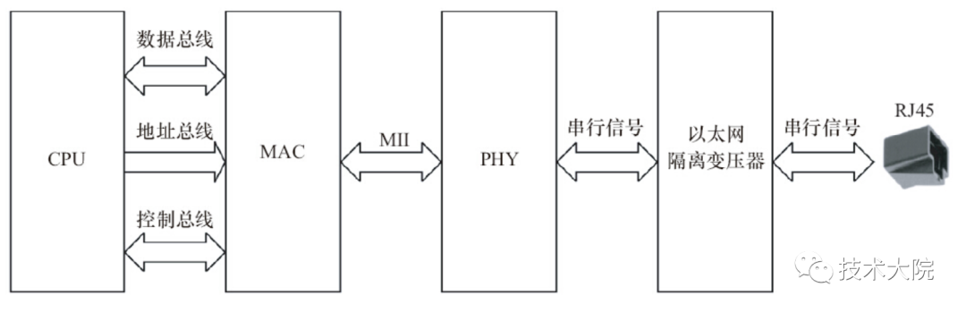
Figure 6 Hardware Circuit Principle of Ethernet Interface
Common Ethernet Interface Types:
-
SC Fiber Optic Port: Higher cost, commonly used in gigabit networks
-
RJ-45 Interface
-
The most common network device interface, commonly known as “crystal head”
-
Requires at least the use of category 5 cable; for stable high-speed, category 6 cable is needed
-
FDDI Interface
-
Fiber transmission, large capacity, long transmission distance, strong anti-interference ability
-
Commonly used in metropolitan area networks, backbone networks in campus environments, and multi-building network distribution environments
-
AUI Interface: Specifically used for connecting thick coaxial cables, now less common
-
BNC Interface
-
Separated display signal interface
-
No longer used in switches
-
Console Interface
-
Generally, Ethernet switches for network management have a “Console” port, specifically used for configuring and managing the switch
-
The most common and basic port for switch management and configuration
PCI and PCIe
PCI (Peripheral Component Interconnect): A local bus introduced by Intel in 1991, serving as a general bus interface standard, widely used in current computer systems.
PCI Features:
-
The data bus is 32 bits, expandable to 64 bits
-
Supports burst mode transmission
-
Indicates continuous transmission of multiple data after obtaining bus control
-
Only the destination’s starting address needs to be provided; after accessing the first data, the second to nth data will be automatically addressed and transmitted based on certain rules
-
In contrast to burst mode is single-cycle mode, which transmits only one data in one bus cycle
-
Bus operation and processor-memory subsystem operations are parallel
-
Uses centralized bus arbitration
-
Supports full automatic configuration and resource allocation; PCI cards contain a group of device information registers to provide information to the system, enabling plug-and-play
-
PCI bus specifications are independent of microprocessors, offering good universality
-
PCI devices can fully act as master devices controlling the bus
A typical 33MHz PCI bus system is shown in the figure above:7:
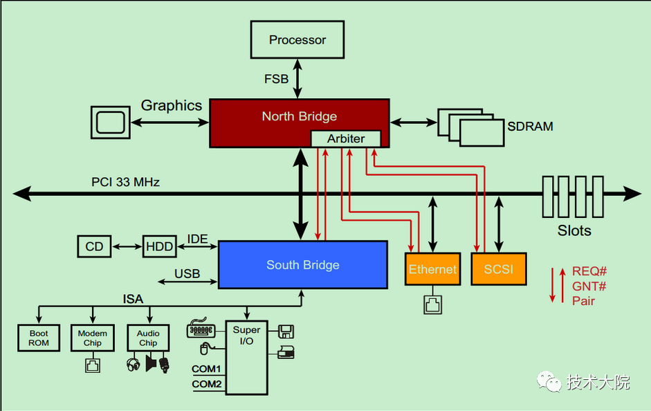
Figure 7 PCI Bus System
-
The processor connects to the north bridge via FSB; the north bridge is mounted with a graphics accelerator (graphics card), SDRAM (memory), and PCI bus
-
The PCI bus is mounted with the south bridge, Ethernet, SCSI bus (an older small computer bus), and several PCI slots
-
CD and hard drives connect to the south bridge via IDE, while audio devices, printers, mice, and keyboards also connect to the south bridge
-
The south bridge also provides several USB interfaces
PCI bus is a shared bus, thus requiring a specific arbiter to determine the control rights of the bus at any given time.
This arbiter is generally located in the north bridge, and the arbiter (host) connects to each slave via a pair of pins, REQ# (request) and GNT# (grant).
Note: Not all devices have the capability to become an arbiter or initiator.
The initial PCI bus clock frequency was 33MHz, but with version updates, the clock frequency has gradually increased. However, due to PCI’s use of a Reflected-Wave Signaling signal model, the higher the clock frequency, the lower the maximum load of the bus, as shown in Figure 8:
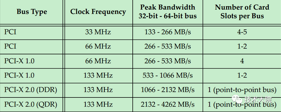
Figure 8 Changes in PCI Clock and Load
PCI Spec specifies that up to 32 PCI devices can be connected to each PCI bus, but in reality, this number is far from 32; a 33MHz 32-bit PCI bus can typically only connect 10 to 12 loads.
Note: If using slots to connect, one connection counts as two PCI devices, with the slot and PCI card each counting as one PCI device. In other words, a 33MHz PCI bus can connect a maximum of 4 to 5 slots or PCI cards.
If more devices need to be connected, PCI bridges can be used to adopt a PCI-to-PCI approach, as shown in Figure 9:
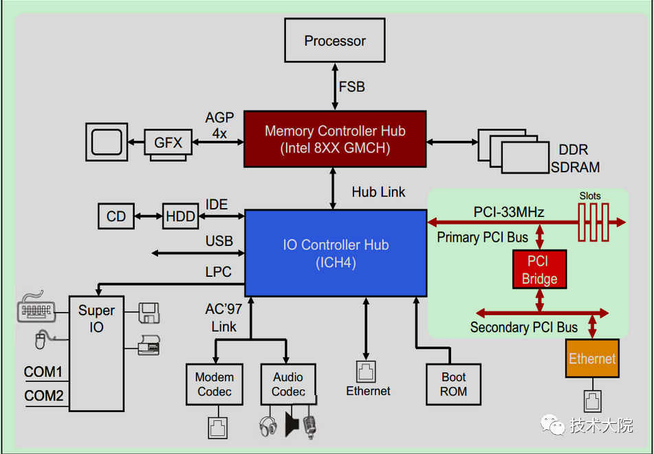
Figure 9 PCI Bus System Including PCI-to-PCI Bridge
To achieve higher bandwidth, the new version of PCI Spec has increased the PCI bus to 64-bit and the frequency to 66MHz, supporting a maximum of 533MB/s, as shown in Figure 10:
Figure 10 Typical 66MHz, 64-bit PCI System Structure
Note:
-
Increasing the bus frequency will inevitably lead to a decrease in bus load capacity
-
A 66MHz 64-bit PCI bus can only support one PCI plug-in device (counted as two PCI devices, the slot and PCI card each count as one)
-
To increase the total number of PCI devices in the system, additional PCI bridges must be added, which further increases power consumption and cost
-
66MHz is basically considered the upper limit of PCI bus frequency
Three Transmission Modes of PCI Bus:
-
Programmed I/O (PIO)
-
Each communication between the CPU and PCI device and SDRAM requires additional clock cycles
-
Also requires long periods of CPU occupation, affecting CPU utilization
-
Peer-to-Peer
-
At least one device capable of becoming a host must exist in the PCI bus system
-
In practical systems, this transmission method is rarely used because the PCI device (Initiator) obtaining host identity and another PCI device (Target) usually adopt different data formats, unless they are from the same manufacturer
-
DMA
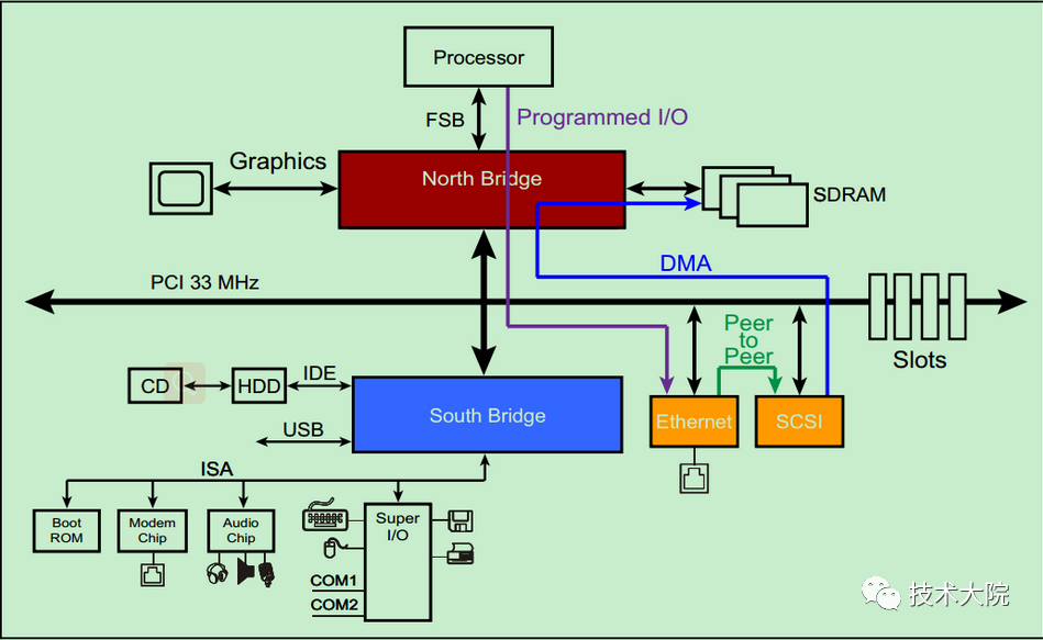
Figure 11 Three Transmission Modes of PCI Bus
PCI-E Bus: A new generation of bus interface proposed by Intel, representing the transition from traditional parallel buses to high-speed serial buses.
PCI-E Features:
-
Uses the currently popular point-to-point serial connection, unlike PCI which shares a bus
-
Transmits data in a serial manner
-
Does not need to request bandwidth from the entire bus
-
Can achieve a very high data transmission rate, reaching a bandwidth that PCI cannot provide
-
Embedded clock technology (Embedded Clock)
-
The sender no longer sends a clock to the receiver, but the receiver can recover the clock from the data lane through 8b/10b encoding
-
PCI Express is software compatible with current PCI technology and devices
Figure 12 PCI-E Connection Diagram
SD and SDIO
SD (Secure Digital): Refers to the commonly seen SD memory card.
-
Designed to be compatible with MMC (Multi-Media Card)
-
SDHC (SD High Capacity) is a high-capacity SD card, supporting a maximum capacity of 32GB
-
SDXC (SD eXtended Capacity), released in 2009, supports a maximum size of 2TB
SDIO (Secure Digital Input and Output Card): A secure digital input/output card, defining peripheral interfaces other than storage cards based on the SD standard.
-
SDIO mainly has two types of applications—removable and non-removable
-
Non-removable devices follow the same electrical standards but do not require compliance with physical standards
-
Many mobile phones or handheld devices now support SDIO functionality to connect WiFi, Bluetooth, GPS, and other modules
Generally, the SD controller integrated within the chip supports both MMC and SD cards, as well as SDIO cards, but the protocols for SD and SDIO differ, and the supported commands may vary.
-
SPI Mode
-
1-bit Mode
-
4-bit Mode
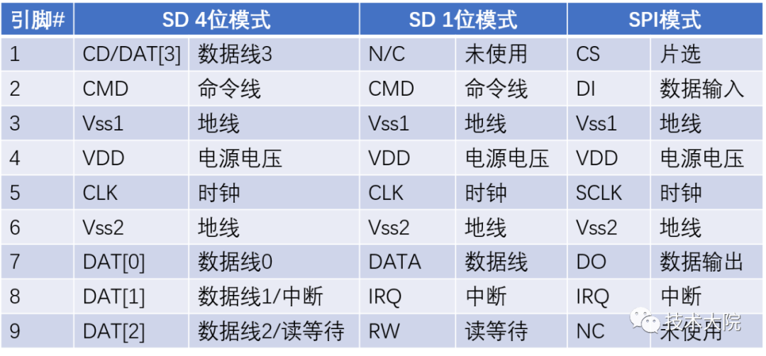
Figure 13 SDIO Interface Pins
Timing:
-
CLK is the clock pin, transmitting one command or data bit per clock cycle
-
CMD is the command pin, where commands are transmitted serially on the CMD line, operating in a bidirectional half-duplex manner (commands from host to card, while responses from the card to the host)
-
DAT[0]~DAT[3] are the data line pins
-
In SPI mode, pin 8 is treated as an interrupt signal

Figure 14 Typical Timing for SDIO Single Module Read
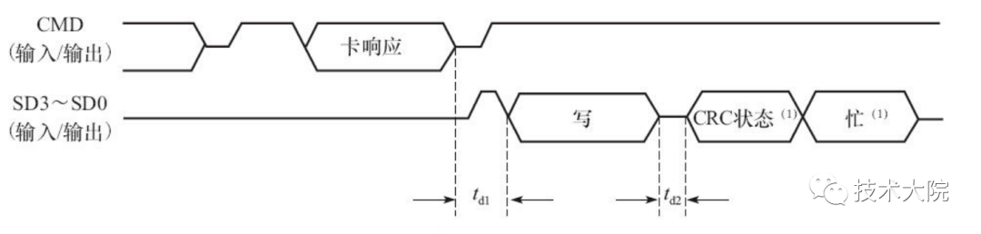
Figure 15 Typical Timing for SDIO Single Module Read and Write
Conclusion