Embedded Developers
Essential Knowledge to Know
Knowledge of ROM, FLASH, and Hard Drive Technology

In embedded development, if the chip has internal Flash, the application program is usually stored in the internal FLASH of the chip, such as in Cortex-M series microcontrollers; if the chip does not have Flash, the application is usually stored in external NAND FLASH, such as in Cortex-A series chips. These Flash can be reprogrammed through software coding.
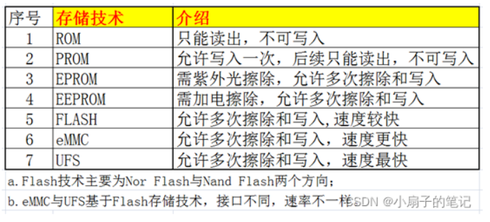
In the early days of computer development, data was stored in ROM, which is read-only and cannot be written, limiting its applications. The emergence of EEPROM and NAND memory later facilitated rapid development in computer storage technology, especially with the high-speed storage technologies eMMC and UFS widely used in the last decade, which have driven rapid advancements in the consumer electronics field, such as the storage technology in smartphones, like the Xiaomi 11 that uses UFS3.1 technology.

Development of Memory

DECEMBER HELLO
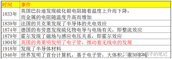
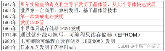
The rapid development of memory is due to the invention and development of semiconductor technology, particularly the invention of transistors and CMOS technology, which control their on/off states through electrical signals, representing 0 and 1 with the opening and closing of switches. These are the basic logical components of storage circuits. With the advent of integrated circuits, ROM storage technology was also born. Here is a brief overview of the history of storage technology:

ROM

DECEMBER HELLO
ROM stands for Read Only Memory, which is a type of memory that is read-only. The programs inside ROM are burned in during the manufacturing process, and the content can only be read and not modified. Once burned in, users can only read the internal data and cannot make any changes. If the content is found to be incorrect, the ROM chip can only be discarded. Because ROM is produced on the production line, and due to high costs, it is generally only used in large-scale applications.

PROM

DECEMBER HELLO
Since ROM is already fixed at the factory, users cannot customize their programs and data, leading to the development of PROM (Programmable ROM). This means that the ROM has no data when it leaves the factory, all bits are set to 1, and users can use specialized tools to burn program data into the ROM. However, this opportunity is only available once; once written, it cannot be modified, and if an error occurs, the written chip can only be discarded.

EPROM

DECEMBER HELLO
PROM, which can only be programmed once, is obviously costly and does not meet development needs, thus leading to the emergence of EPROM (Erasable Programmable ROM). This chip can be erased and rewritten using ultraviolet light, solving the limitation of PROM that can only be written once.
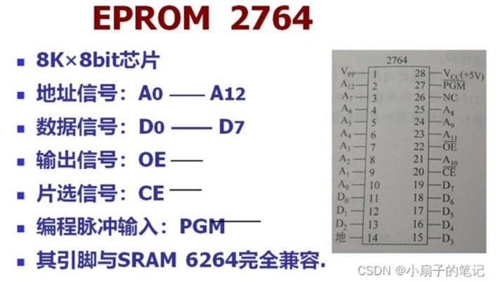
EPROM chips have a distinct feature: there is a glass window on the front of their ceramic packaging, allowing visibility of the internal integrated circuit. Ultraviolet light can erase the internal data through this window, and an EPROM eraser is required to complete the chip erasure operation.
EPROM models start with 27, such as 2764 (8*8K), which is a 64K Bits capacity EPROM chip. After writing the program, the EPROM chip must be covered with an opaque sticker or tape to prevent exposure to surrounding ultraviolet light, which could lead to data loss.
Although EPROM can be erased and reprogrammed multiple times, it still requires a programmer, making it less convenient to use. Therefore, EEPROM (Electrically Erasable Programmable ROM) was subsequently developed. EEPROM can be erased without the aid of other devices; it modifies its content using electronic signals and can be modified in Byte as the smallest unit, eliminating the need to erase and rewrite entirely, making it very suitable for external storage in embedded devices.
EEPROM is still in use today; for example, Atmel’s AT24C series CMOS EEPROM uses IIC communication interface, with a voltage range of 1.8-3.6V, and is widely applied in embedded devices.

Flash

DECEMBER HELLO
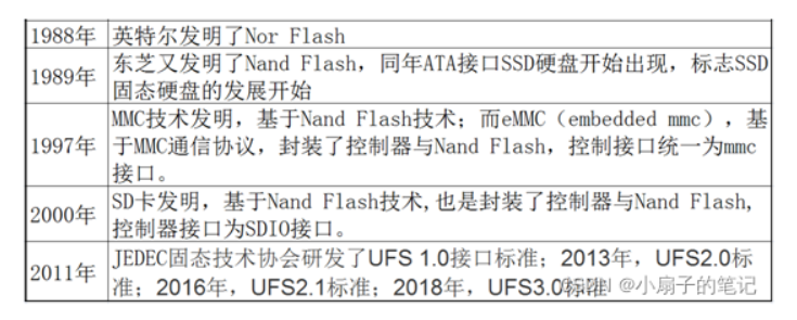
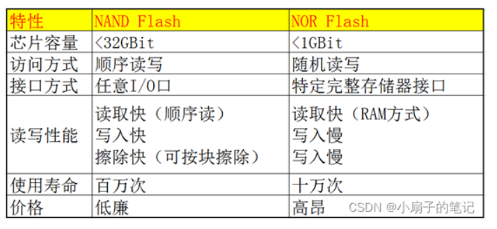
Flash memory is primarily based on NOR flash technology developed by Intel in 1988 and NAND flash technology developed by Toshiba in 1989; their emergence has completely changed the landscape of the memory market, which was previously dominated by EPROM (Erasable Programmable Read-Only Memory) and EEPROM (Electrically Erasable Programmable Read-Only Memory).
The difference between these two technologies lies in the interface and internal storage structure. In terms of interface, NOR flash has independent address and data lines, while NAND flash does not. Their characteristics are shown in the following table:
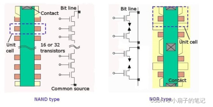
In terms of internal structure (based on SLC NAND), the differences are as follows:
5.1 NOR Flash
The biggest feature of NOR Flash is its support for XIP (Execute In Place), which means that programs can be executed directly in the NOR flash chip without the need for relocation or copying to RAM.
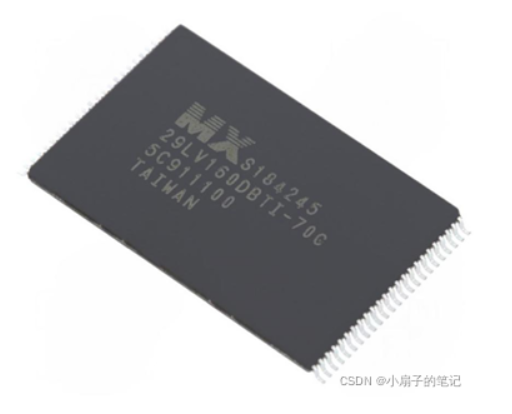
As shown in the figure above, NOR Flash model is MX29LV160.
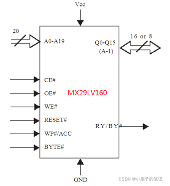
The address and data lines of NOR Flash are separate; as long as the data address is provided, the data bus can correctly provide the data. However, it cannot be directly written to; before executing a write operation, a fixed command sequence must be sent, followed by the address and data for the write operation.
The minimum access units of NOR Flash memory are generally divided into 8-bit and 16-bit, and some NOR Flash devices support both 8-bit and 16-bit modes. This Flash’s bit width can be selected when designing hardware. When the chip’s BYTE# pin is high, the chip operates in 16-bit mode; when the BYTE# pin is low, the chip operates in 8-bit mode.
NOR Flash typically has multiple sectors, with sectors being the minimum unit of erasure. The size of each sector in NOR Flash is not fixed.
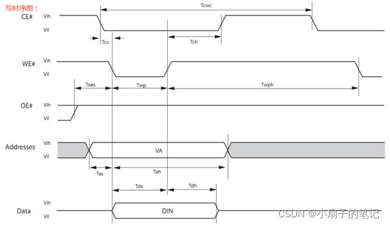
Taking MX29LV160 as an example, the write timing diagram is shown below (address and data buses are independent):
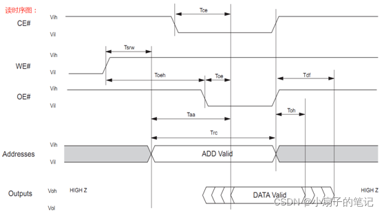
The read timing diagram is shown below; for specifics, refer to the data manual:
5.2 NAND Flash
5.2.1 NAND Types
NAND flash is currently the most widely used flash memory technology. Mainstream products like SD cards, eMMC, UFS, SSD, etc., are all based on NAND flash technology. However, NAND flash can be categorized based on its storage cell types into SLC, MLC, TLC, QLC, PLC, and many more types in the LC series that will emerge in the future. The differences between these types lie in the number of bits that a single storage cell can represent, as illustrated in the following diagram:
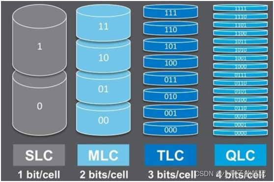
SLC: One cell represents 1 bit of data;
MLC: One cell represents 2 bits of data;
TLC: One cell represents 3 bits of data;
QLC: One cell represents 4 bits of data;
Thus, NAND flash of the same size can store four times the capacity when based on QLC compared to SLC. However, despite the increased storage capacity, the read/write speed, erase lifespan, and stability are lower. Currently, most products in the market are based on SLC, MLC, and TLC cell structures, with the following comparative characteristics:
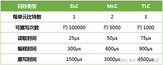
SLC is fast to read/write, has a long lifespan, but is expensive and has low capacity; while TLC is slow to read/write, has a short lifespan, but is cheap and has high capacity. Therefore, among NAND flash-based products on the market, low-end products are mostly TLC, mid-range products are mostly MLC, and high-end enterprise products use SLC, focusing on stability.
5.2.2 2D and 3D Technology
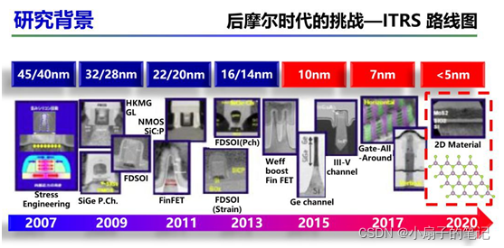
The current market pursues miniaturization of devices while maximizing capacity; thus, through continuous improvement of process technology, the size of each storage cell is reduced, such as from 45nm to 16nm (the most advanced process currently is Qualcomm’s Snapdragon 888 processor at 5nm), achieving expanded storage capacity within the same chip volume.
However, the improvement of the process also brings a bottleneck; as the process technology improves and the size of each storage cell decreases, the oxide layer of NAND cell particles becomes thinner, leading to lower reliability, especially for QLC, where one storage cell represents 4 bits of data, the impact is greater.
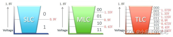
Assuming the storage cell voltage is 1.8V, for SLC, one bit has two states, averaging 1.8V voltage, with each state getting 0.9V; for MLC, four states average the voltage, with each state getting 0.45V; and so forth. For TLC, each state can only get 0.225V, while QLC is even worse, with each state only getting 0.1125V. At such low voltages, having so many states with such small voltage separations makes it increasingly difficult to control, and the interference becomes more complex, affecting the performance, reliability, and stability of TLC or QLC flash memory.
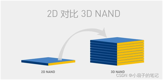
NAND 2D technology belongs to the category of planar flash memory, with its capacity bottleneck at 10/9nm. Therefore, NAND 3D technology was proposed as early as 2007, which is a three-dimensional structured flash memory. To illustrate: if 2D is a bungalow, then 3D is a skyscraper, with 3D being a stack of N levels of 2D flash, as shown in the figure above.
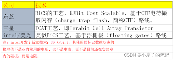
However, 3D is not simply stacking; different companies have different 3D processing technologies. In 3D flash memory, representative processes include:
It is precisely because of the 3D NAND technology that some TLC products using this technology have achieved MLC performance, which is commonly referred to as 3D TLC. Additionally, major manufacturers like Samsung and Micron have already launched their fourth-generation 3D QLC products into the market, allowing consumers to experience higher capacities, lower prices, and faster read/write performance.
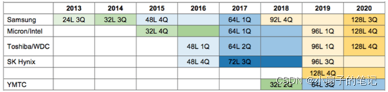
With the advent of 3D NAND, 2D has reached its limits due to the bottleneck of not being able to shrink cell sizes further. The latest 3D stacking layers have reached 128 layers, as shown in the figure below:
5.2.3 NAND Interface and Timing
NAND flash is faster in writing/erasing than NOR flash, has a longer lifespan, and is more cost-effective, leading to broader applications. However, it does not have independent address and data buses; the address and data share 8bit/16bit IO, so its read rate is slightly lower than NOR.
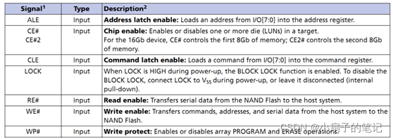
For example, Micron’s MT29F series NAND flash (such as MT29F16G08) uses multiplexed 8bit or 16bit IO for command, address, and data transmission, along with five control signals CE#, CLE, ALE, WE#, RE#, and WP for write protection and R/B status signal lines.
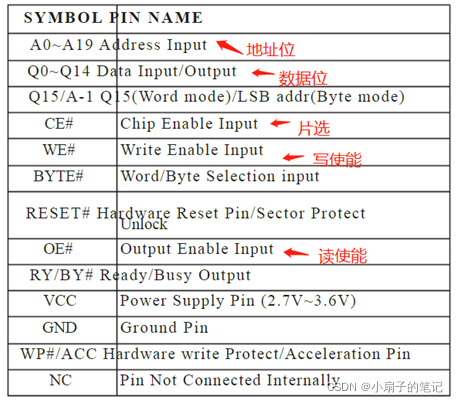
The functions of each pin are described in the table below:
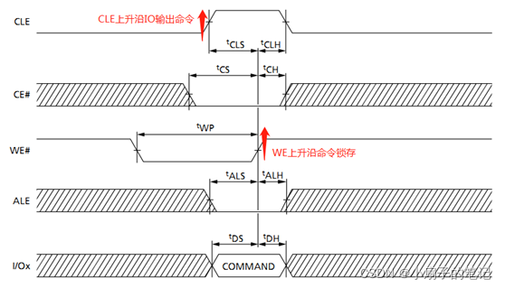
Writing command timing:
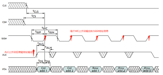
Address writing timing:
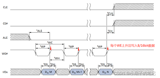
Data writing timing:
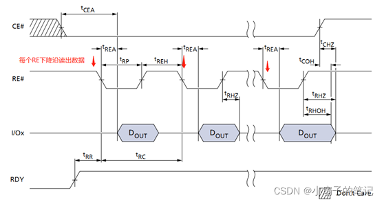
Data reading timing:
The specific commands and address information for reading and writing the MT29F series chips can be referenced in the MT29F series specification; the link is:
Link:
https://pan.baidu.com/s/15SHhADiX1uD4CCDA20nXvQ
Extraction code: d80g