First, we need to ask, what is signal integrity? Why do we perform signal integrity analysis? How do we conduct signal integrity analysis? What do we achieve after signal integrity analysis?Let’s first discuss,what is signal integrity?Signal Integrity (SI): It refers to the ability of a signal to be transmitted and switched in a circuit with the correct timing, levels, and waveforms. It is a very important concept in high-speed circuit design, primarily focusing on whether the signal can maintain its integrity and accuracy during transmission, thereby ensuring the reliability and performance of the circuit system.To conclude: There are no impedance requirements for SPI routing.Of course, you can adjust the trace dimensions of the SPI bus to achieve a 50-ohm impedance, but this is not necessary. SPI does not specify any particular impedance requirements. If you look at other design guidelines that claim “SPI requires controlled impedance,” you will find that they typically do not specify a specific impedance value. At most, they provide a range of 30 ohms to 150 ohms. However, this is not the same concept as the trace impedance, and the effects are different.In fact, impedance control for SPI lines is only necessary when the interconnect length becomes very long. Moreover, since the bus does not have specific impedance requirements, you have some freedom in channel design and termination.So,what exactly qualifies as “very long”? When is a certain termination method required?SPI Topology and Routing Design The topology of SPI is very simple. If there are multiple slave devices on the bus, four lines are used to connect a single controller-peripheral link. The upstream controller can send and receive data at rates of up to 60 Mbps over a pair of lines, and the data may also be sent via cables to another circuit board or device. A typical SPI bus topology is shown below.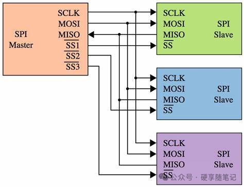 So what happens on the PCB? If you look at the datasheet of components with SPI interfaces, you will find that the minimum rise time value for advanced components can be as short as 1 ns. For some components, the rise time may be longer, reaching 20 ns or even longer. Therefore, while SPI is understood as a slow bus, its rates are not low; it’s just that the rates may not be high when we use it. Once we look at the rising and falling edges, even waveforms at tens of kHz can become high-speed signals. In a previous project, we used an FPGA to generate raw waveforms, then converted them into square waves, and used RC delay to compare two waveforms, ultimately producing a 2 ns pulse waveform to drive a laser.So, what is the best approach for SPI design? What is the rise time in SPI routing?The first step is to check the datasheet to find the main component controlling the SPI bus. If your component has detailed documentation, the rise time of the SPI interface will be specified based on the specificload capacitanceon the bus. Note that the “load capacitance” assumes zero connection inductance between the SPI output and the test load, so you can consider this rise time value as a first-order approximation of the RC time constant.
 Example datasheet entries involve rise and fall times specified for a specific load capacitance.In the above example, the high load capacitance value is not typical for most components, but it illustrates a key point: the rise time is determined by the bus capacitance. In this case, if we take the specified 10%-90% rise time and set it equal to 2.2RC (2.2RC is derived from the step response of a first-order RC circuit. When an RC circuit charges, the time for the voltage to rise from 10% to 90% is approximately 2.2RC), which means 2.2RC=10 ns; we will get R = 113.6, which is the resistance on the bus. In other words, the larger the impedance, the longer the rise time, so we often use this method to slow down the rising edge. Whether in serial communication or other buses, a relatively small resistor is often placed in series to slow down the rising edge.Is the SPI bus long or short?There is a rule of thumb: if the time it takes for a signal to propagate back and forth on the bus (round-trip delay) is less than a certain proportion of the signal rise time, it can be considered a “short bus.” However, this rise time is not explicitly defined; some take 10% rise time, 20% rise time, and some take 50% rise time. Here we conservatively take 10% rise time. That is:
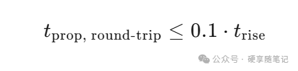 The typical dielectric constant for commonly used FR4 substrates is 4 (Dk=4). On the PCB, the signal propagation speed is determined by the relative dielectric constant (Dk or εᵣ) of the PCB material and structure, not the speed of light;The formula
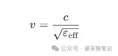 c is the speed of light in a vacuum, εeff is calculated as 4, substituting into the formula gives v=1.5*10⁸ m/s, with a 10% rise time of 1 ns;If we calculate the transmission time as 10 ns, L is the length, and the signal travels back and forth, which is 2L,2L=1.5*10⁸*1*10⁻⁹L=0.075 mAfter conversion, L=75 mm;This applies to most situations. In other words, when the SPI trace is longer than 75 mm, it is considered long; when the trace is within 75 mm, the SPI bus is short.Why do people declare or use 50 ohms in SPI?In cases where specific impedance is required for SPI lines, if 50 ohms is the target characteristic impedance for the electrical length of the SPI bus, then there are likely other impedance-controlled traces on the circuit board also targeting 50 ohms. A single impedance target makes it easier for manufacturers to control impedance. If they have to change materials in the stack-up to achieve the impedance target, it is much easier to operate if there is only one target to meet. In simple terms, it depends on whether there are other impedance lines on your PCB; it’s best to synchronize with others as much as possible.Why use series termination on short SPI buses?From the above, we can see that in the vast majority of practical cases of using SPI traces, drivers or receivers do not require termination. If needed, you will see impedance specifications in the component datasheet, SPI specifications, or both. Additionally, the components are likely already designed with on-chip termination for the target impedance, so you do not need to place resistors with effort.
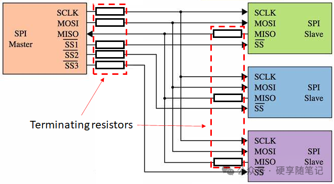 Termination resistors placed on the SPI bus.The answer is simple:It is toslow down the signals emitted by the driver. The resistors also have the added benefit ofsuppressing ringing at the output. It is important to note that in this case,the choice of resistor is not related to impedance matching in electrical short lines.If your controller is a high-level component like an FPGA, and you instantiate an SPI interface within that controller, then the rise time may be very short because the physical structure of the device itself ensures very fast rise times. Therefore, slowing down the signal speed to avoid crosstalk from fast signals may be beneficial. In this case,the resistor must be placed close to the driver, as this will ensure reduced crosstalk across the entire line. Be careful not to slow down the rise time too much, or the signal speed may be too slow to switch the I/O on the load, and the signal may not be read correctly. If the rise time is too long, it may also violate the setup time.——————————————————END——————————————————