01
eMMC Signal Impedance and Routing
-
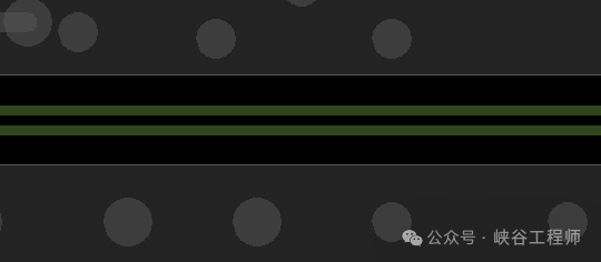
It is recommended to use ground wrapping for CLK and STRB signals, with a ground via every ≤500 mil.

-
During overall layout,eMMC should be placed as close to the SOC as possible to minimize routing length.
-
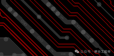
The reference layer for all eMMC signals must be a complete ground plane to avoid interruptions in the return path due to continuous vias.
-
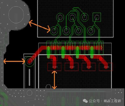
The 22-ohm series matching resistor for CLK should be placed close to the CPU end (source end), and the routing between the CPU pin and the resistor must be controlled within 300 mil.
-
The 0-ohm series matching resistor for STRB should be placed close to the eMMC chip end, and the routing between the eMMC pin and the resistor must be controlled within 300 mil.
-
The external capacitor for the VDD pin must be placed close to the corresponding pin, with routing kept as short and wide as possible.
|
Serial Number |
Routing Parameters |
Routing Requirements |
|
1 |
Routing Impedance |
Single-ended50 ohm ±10% |
|
2 |
Clock (CLK, STRB) and data must be of equal length |
<120 mil |
|
3 |
Routing Length |
<3 inches |
|
4 |
Spacing between eMMC signal lines |
2 times the eMMC line width |
|
5 |
Spacing between eMMC and other signals |
3 times the line width, at least 2 times the eMMC line width |
|
6 |
Allowed number of vias for each signal |
Generally no more than2 |
02
USB2.0 Interface Circuit Routing
-
During overall layout,the USB connector should be placed as close to the SOC as possible to minimize routing length.
-
USB differential pairs should ideally reference a complete ground plane and require full ground wrapping, with ground vias within 300 mil.
-
When routing USB differential signals across layers, ensure the number of vias on the routing is less than 4, not exceeding 6, and place symmetrical stitching ground vias close to the signal vias, with a center distance of no more than 30 mil.
|
Serial Number |
Routing Parameters |
Routing Requirements |
|
1 |
Routing Impedance |
Differential90 ohm ±10% |
|
2 |
Equal length for differential pairs |
<20 mil |
|
3 |
Routing Length |
<6 inches |
|
4 |
Allowed number of vias for each signal |
It is recommended not to exceed4, not to exceed 6 |
03USB3.0 Interface Circuit Routing
-
During overall layout,the USB connector should be placed as close to the SOC as possible to minimize routing length.
-
The decoupling capacitor for the power supply must be placed close to the corresponding power pin.
-
SSTXP/N and SSRXP/N should ideally be routed on the TOP layer, and if layer change is necessary, it must not exceed2 vias, with symmetrical stitching ground vias placed close to the signal vias, and the center distance between stitching ground vias and signal vias must not exceed30 mil, and routing corners should preferably use arcs or obtuse angles, not right or acute angles.
-
STXP/N, SSRXP/N signal reference layers need to be complete ground planes to avoid interruptions in the return path due to continuous vias.
-
USB3.0 interface signals should be fully ground wrapped, with a ground via every ≤300 mil. USB3.0 signals need to reference a complete GND plane.
|
Serial Number |
Routing Parameters |
Routing Requirements |
|
1 |
Routing Impedance |
Differential90 ohm ±10% |
|
2 |
Equal length requirement for differential pairs |
<6 mil |
|
3 |
Routing Length |
Host device<6 inches, Device and OTG device<5 inches |
|
4 |
Capacitance Requirements |
100nF ±20%, recommended to use 0201 package |
|
5 |
Spacing between differential pairs |
Greater than or equal to4 times USB line width |
|
6 |
Spacing between USB and other signals |
Greater than or equal to4 times USB line width |
|
7 |
Allowed number of vias for each signal |
It is recommended not to exceed2 |
|
8 |
ESD Requirements |
I/O to ground capacitance not exceeding 0.2pF |
04MIPI CSI/DSI Interface Circuit Routing
-
During overall layout,the USB connector should be placed as close to the SOC as possible to minimize routing length.
-
The decoupling capacitor for the power supply must be placed close to the corresponding power pin.
-
Minimize layer change vias; if layer change is necessary, it is recommended not to exceed4 vias, and place symmetrical stitching ground vias close to the signal vias, with a center distance of no more than30 mil..
-
It is recommended to fully ground wrap MIPI signal pairs, with a ground via every ≤500 mil. MIPI signals need to reference a complete GND plane.
-
The reference layer for MIPI CSI differential pairs needs to be a complete ground plane to avoid interruptions in the return path due to continuous vias.
|
Serial Number |
Routing Parameters |
Routing Requirements |
|
1 |
Routing Impedance |
Differential100 ohm ±10% |
|
2 |
Equal length requirement for differential pairs |
<12 mil |
|
3 |
Equal length requirement between data and clock differential pairs |
<36 mil |
|
4 |
Spacing between differential pairs |
Greater than or equal to3 times the line width |
|
5 |
Spacing between MIPI and other signals |
Greater than or equal to3 times the line width |
|
6 |
Allowed number of vias for each signal |
It is recommended not to exceed4 |
|
7 |
Routing Length |
<6 inches |
05
LVDS Interface Circuit Routing
-
During overall layout,the USB connector should be placed as close to the SOC as possible to minimize routing length.
-
The decoupling capacitor for the power supply must be placed close to the corresponding power pin.
-
For LVDS differential pairs, minimize layer change vias; if layer change is necessary, it is recommended to have less than4 vias, not exceeding6 vias, and place symmetrical stitching ground vias close to the signal vias, with a center distance of no more than30 mil..
-
It is recommended to fully ground wrap LVDS signal pairs, with a ground via every ≤600 mil. LVDS signals need to reference a complete GND plane.
-
The reference layer for LVDS differential pairs needs to be a complete ground plane to avoid interruptions in the return path due to continuous vias.
|
Serial Number |
Routing Parameters |
Routing Requirements |
|
1 |
Routing Impedance |
Differential100 ohm ±10% |
|
2 |
Equal length requirement for differential pairs |
<12 mil |
|
3 |
Equal length requirement between data and clock differential pairs |
<60 mil |
|
4 |
Routing Length |
<6 inches |
|
5 |
Spacing between differential pairs |
Greater than or equal to3 times LVDS line width |
|
6 |
Spacing between LVDS and other signals |
Greater than or equal to3 times LVDS line width |
|
7 |
Allowed number of vias for each signal |
Not exceeding4 |
06
RGMII Interface Circuit Routing
-
It is recommended to use ground wrapping for the CLK signal, with a ground via every ≤500 mil.
-
During overall layout,the USB connector should be placed as close to the SOC as possible to minimize routing length.
-
The decoupling capacitor for the power supply must be placed close to the corresponding power pin.
-
The 22-ohm series matching resistor for ETH_CLK_25M should be placed close to the CPU end (source end), and the routing between the CPU pin and the resistor must be controlled within 400 mil.
-
ETH_CLK_25M must be fully ground wrapped, with ground vias within 300 mil.
-
MII mode MCLKINOUT input mode: the 22-ohm series matching resistor should be placed close to the PHY end, and the routing between the PHY pin and the resistor must be controlled within 400 mil.
-
All RGMII/RMII signals must reference a complete ground plane to avoid interruptions in the return path due to continuous vias.
-
The network transformer should be placed as close as possible to the RJ45 connector, and the MDI routing must not exceed4.5 inches.
-
The differential signal differential impedance from PHY to the network transformer should be100Ω ±10%.
-
The differential signals from PHY to the network transformer, including MDI0+, MDI0-, MDI1+, MDI1-, MDI2+, MDI2-, MDI3+, and MDI3-, should have a length deviation controlled within ±5 mil, and MDI differential pairs must strictly follow differential routing rules.
-
The spacing between MDI0/1/2/3 should be ≥3 times the line width.
-
The spacing between MDI0/1/2/3 and other signals should be ≥4 times the line width.
-
Minimize layer change vias; if layer change is necessary, it should not exceed2 vias, and place symmetrical stitching ground vias close to the signal vias.
-
The differential pairs on the high voltage side of the network transformer should have a routing width as wide as possible, recommended to be8 mil.
-
The center-tap filter capacitor of the network transformer must be placed close to the corresponding pin of the network transformer.
-
The decoupling capacitors for the HY chip power supply must be placed as close as possible to each PHY chip pin, with routing going through the capacitor pad before reaching the chip pin, and the routing length between the pin and the capacitor must not exceed100 mil.
-
All components on the high voltage side of the network transformer must be kept away from the main ground of the PCB.
-
The RJ45 interface and the high voltage side of the network transformer belong to the high voltage area, and copper covering is prohibited; it is recommended to maintain a distance of at least4mm or more.
|
Serial Number |
Routing Parameters |
Routing Requirements |
|
1 |
Routing Impedance |
Single-ended50 ohm ±10% |
|
2 |
(TXD{0-3}, TXEN) to TXCLK equal length |
<120 mil |
|
3 |
(RXD{0-3}, RXDV) to RXCLK equal length |
<120 mil |
|
4 |
Routing Length |
<6 inches |
|
5 |
Spacing between RGMII signal lines |
≥2 times RGMII line width |
|
6 |
Spacing between RGMII and other signals |
3 times RGMII line width, at least 2 times RGMII line width |
|
7 |
Allowed number of vias for each signal |
It is recommended not to exceed2 |
07
WIFI/BT Circuit Routing
-
During overall layout, the WIFI module should be placed appropriately, keeping it away from DDR, HDMI, USB, LCD circuits, and other easily interfered modules or connectors.
-
The TOP layer below the module should not have routing, ensuring a complete ground plane as the reference plane, and SDIO/PCIe/UART/PCM signal lines should be routed around the module projection area before connecting to the module pins.
-
Crystal circuit layout should be prioritized, and should be placed on the same layer as the chip and as close as possible to avoid vias; crystal routing should be kept as short as possible, away from interference sources, preferably in the antenna area.
-
Both the crystal and clock signals need to be fully ground wrapped, with a ground via added at least every100 mil, and it must ensure that the ground reference plane of the adjacent layer is complete.
-
When laying out the inductance of the module, ensure that the routing goes through the capacitor before entering the module power pin.