When connecting a microcontroller to sensors, displays, or other modules, have you ever considered how the two devices communicate? What exactly are they saying? How can they understand each other?
Communication between electronic devices is like communication between humans; both parties need to speak the same language. In electronics, these languages are called communication protocols.
Let’s first understand the basics of the three most common protocols: Serial Peripheral Interface (SPI), Inter-Integrated Circuit (I2C), and Universal Asynchronous Receiver/Transmitter (UART) driven communication.
SPI, I2C, and UART are much slower than protocols like USB, Ethernet, Bluetooth, and WiFi, but they are simpler and use less hardware and system resources. SPI, I2C, and UART are very suitable for communication between microcontrollers and between microcontrollers and sensors, where there is no need to transmit large amounts of high-speed data.
Serial and Parallel Communication
Electronic devices communicate with each other by sending data bits over wires connected between them, somewhat like letters in an alphabet, except that a bit is binary, meaning it can only be 1 or 0. Bits are transmitted from one device to another through rapid changes in voltage. In a system operating at 5V, a 0 bit is communicated as a short pulse of 0V, while a 1 bit is communicated as a short pulse of 5V.
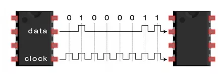
Data bits can be transmitted in parallel or serial form. In parallel communication, data bits are sent simultaneously, each through a separate line. The following diagram shows the parallel transmission of the letter “C” in binary (01000011):
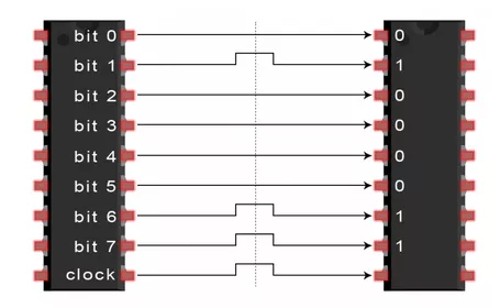
In serial communication, these bits are sent one by one over a single wire. The following diagram shows the serial transmission of the letter “C” in binary (01000011):
SPI, short for Serial Peripheral Interface, is a synchronous communication protocol first defined by Motorola for its MC68HCXX series processors. The SPI interface is primarily used between EEPROM, FLASH, real-time clocks, AD converters, and digital signal processors and decoders. SPI is a high-speed, full-duplex, synchronous communication bus that only occupies four pins on the chip, saving the chip’s pins and providing convenience for PCB layout. Due to its simplicity and ease of use, more and more chips are integrating this communication protocol.
1. Features of SPI
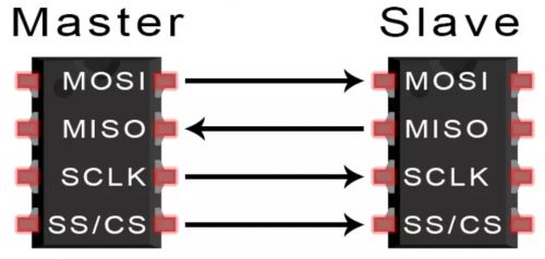
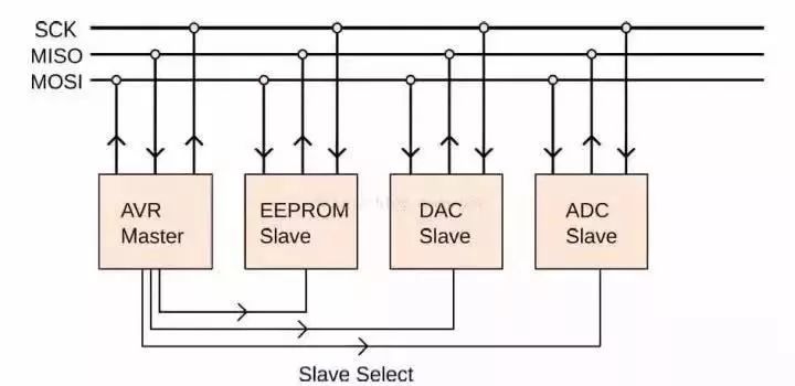
(1) Master-Slave Control Mode
SPI specifies that communication between two SPI devices must be controlled by a master device. A master device can control multiple slave devices by providing the clock and selecting the slave device. The clock for the slave device is provided by the master device through the SCK pin, and the slave device cannot generate or control the clock. Without a clock, the slave device cannot function properly.
(2) Synchronous Data Transmission
The master device generates corresponding clock pulses based on the data to be exchanged, forming a clock signal that controls when data is exchanged and when received data is sampled, ensuring that data is transmitted synchronously between the two SPI devices.
(3) Data Exchange
The data transfer between SPI devices is referred to as data exchange because the SPI protocol specifies that a SPI device cannot simply act as a “transmitter” or “receiver” during data communication. During each clock cycle, SPI devices send and receive one bit of data, effectively exchanging one bit of data. A slave device must be accessed by the master device to receive control signals sent by the master. Therefore, the master device must first select the slave device using the SS/CS pin before accessing it. During data transmission, each received data must be sampled before the next data transmission. If the previously received data is not read, it may be discarded, causing the SPI physical module to fail. Therefore, in programs, it is common to read the data from the SPI device after the SPI transmission is complete, even if this data (dummy data) is useless in the program.
(4) Four Transmission Modes of SPI
Rising edge, falling edge, leading edge, and trailing edge trigger. There are also MSB and LSB transmission methods.
(5) Only Master and Slave Modes
There is no distinction between reading and writing because, in essence, each SPI communication involves data exchange between master and slave devices. This means that sending data will inevitably receive data; to receive data, one must first send data.
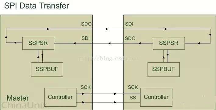
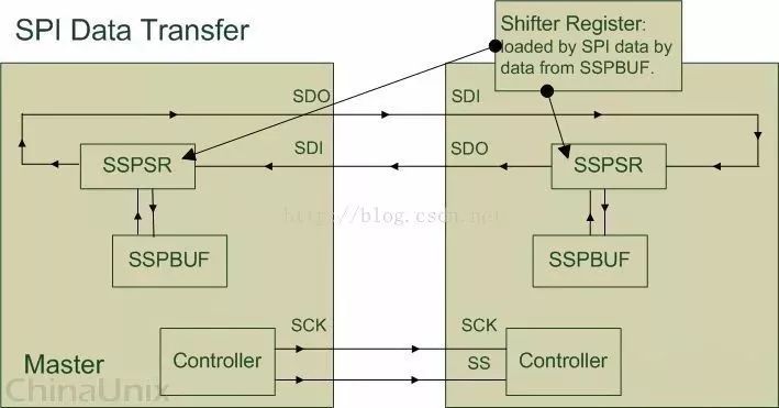
(1) Overview
The above image is a simple description of communication between SPI devices; below we will explain several components shown in the diagram:
SSPBUF, Synchronous Serial Port Buffer, generally refers to the internal buffer of the SPI device, which is usually in FIFO form, storing temporary data during transmission;
SSPSR, Synchronous Serial Port Register, refers to the shift register inside the SPI device, which moves data in or out of SSPBUF according to the set bit-width;
Controller, refers to the control register inside the SPI device, which can configure the transmission mode of the SPI bus.
Typically, we only need to program the four pins described in the above image to control data communication between SPI devices:
SCK, Serial Clock, mainly transmits the clock signal from the master device to the slave device, controlling the timing and rate of data exchange;
SS/CS, Slave Select/Chip Select, used by the master device to select the slave device, allowing the selected slave device to be accessed by the master device;
SDO/MOSI, Serial Data Output/Master Out Slave In, also known as Tx-Channel on the master, serves as the data output for sending data from the SPI device;
SDI/MISO, Serial Data Input/Master In Slave Out, also known as Rx-Channel on the master, serves as the data input for receiving data from the SPI device;
During communication, a data loop is formed between the master and slave devices, as illustrated above, where data is moved in and out of SSPBUF controlled by SSPSR, and the controller determines the communication mode of the SPI bus, while SCK transmits the clock signal.
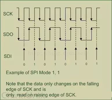
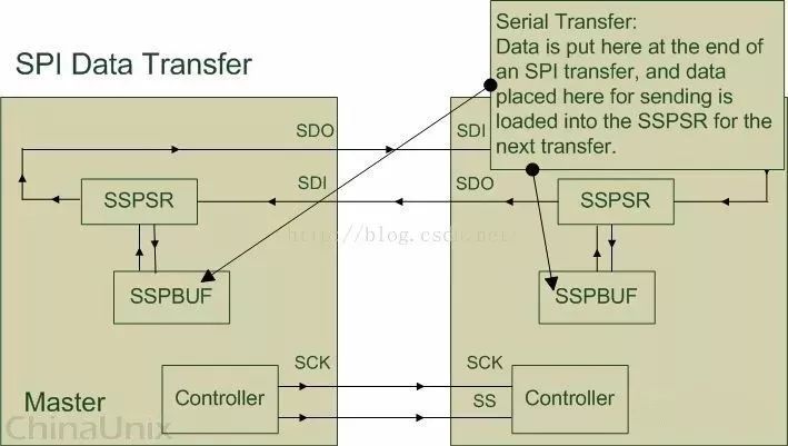
(2) Timing
The above image illustrates the SPI protocol’s working mechanism by exchanging 1 Byte of data between the master and slave devices. First, let’s explain the concepts of phase and polarity.
a. SPI Related Abbreviations or Terms
The polarity (CPOL) and phase (CPHA) of SPI are commonly referred to as CKPOL (Clock Polarity) and CKPHA (Clock Phase), but other notations exist. Here is a simple summary:
(1) CKPOL (Clock Polarity) = CPOL = POL = Polarity = (Clock) Polarity(2) CKPHA (Clock Phase) = CPHA = PHA = Phase = (Clock) Phase(3) SCK=SCLK=SPI Clock(4) Edge = The moment when the clock level changes, either rising edge or falling edge.
Within a clock cycle, there are two edges, referred to as:
Leading edge = First edge; if the starting voltage is 1, it’s when it changes from 1 to 0; if the starting voltage is 0, it’s when it changes from 0 to 1;
Trailing edge = Second edge; if the starting voltage is 1, it’s when it changes from 0 to 1 (after the first change from 1 to 0, the second change can occur); if the starting voltage is 0, it’s when it changes from 1 to 0;
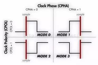
b. SPI Phase and Polarity
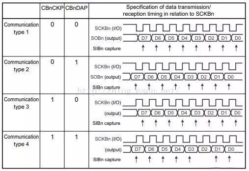
CPOL and CPHA can each be 0 or 1, corresponding to four combinations:Mode 0 CPOL=0, CPHA=0Mode 1 CPOL=0, CPHA=1Mode 2 CPOL=1, CPHA=0Mode 3 CPOL=1, CPHA=1
c. CPOL Polarity
First, let’s define the idle state of the SCLK clock, which is the state before and after sending 8 bits of data. The corresponding state during data transmission is the active state.
In English, it can be simplified as: Clock Polarity = IDLE state of SCK.Now in detail:
CPOL indicates whether the idle state of SCLK is low (0) or high (1):CPOL=0 indicates that the idle state is low, meaning when SCLK is active, it’s high (active-high);
CPOL=1 indicates that the idle state is high, meaning when SCLK is active, it’s low (active-low);
d. CPHA Phase
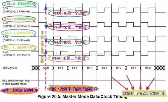
Firstly, capture strobe = latch = read = sample, all represent data sampling, the moment the data is valid. The phase corresponds to which edge (first or second) the data is sampled. 0 corresponds to the first edge, while 1 corresponds to the second edge.
For:CPHA=0 indicates the first edge:For CPOL=0, when idle is low, the first edge is from low to high (rising edge);For CPOL=1, when idle is high, the first edge is from high to low (falling edge);CPHA=1 indicates the second edge:For CPOL=0, when idle is low, the second edge is from high to low (falling edge);For CPOL=1, when idle is high, the first edge is from low to high (rising edge);It might be easier to understand with the above diagram.
e. How to Set SPI Polarity and Phase in Software
SPI consists of master and slave devices, which communicate through the SPI protocol.Setting the SPI mode of the slave device determines the mode of the master device.Therefore, one must first understand the SPI mode of the slave device and then set the master device’s SPI mode to match that of the slave for normal communication.
For the slave device’s SPI mode, there are two types:
Fixed, determined by the SPI slave hardware
The specific SPI mode of the slave device will be described in the related datasheet, which you need to find:
For the SPI slave device, whether it is high or low when idle determines whether CPOL is 0 or 1;Then find out whether the device samples data on the rising or falling edge, which allows for determining CPHA based on the established CPOL value.
Configurable, set by software
The slave device is also an SPI controller, supporting all four modes; one can simply set it to a desired mode.Once the slave device’s mode is known, the master device’s mode can be set to match the slave device’s mode for communication.As for how to configure the CPOL and CPHA of SPI, it is usually done by writing 0 or 1 to the corresponding registers in the SPI controller.
SSPSR is the shift register inside the SPI device. Its main function is to move data in or out of SSPBUF based on the state of the SPI clock signal. The size of data moved each time is determined by Bus-Width and Channel-Width.
The Bus-Width specifies the unit of data transmission between the address bus and the master device.
For example, if we want to write 16 Bytes of data to the SSPBUF of the master device: First, set the Bus-Width of the master device’s configuration register to Byte; then write data to the Tx-Data shift register at the address bus entry, writing 1 Byte of data at a time (using the writeb function); after writing 1 Byte of data, the Tx-Data shift register of the master device will automatically move the 1 Byte of data from the address bus into the SSPBUF; this action needs to be repeated 16 times.
The Channel-Width specifies the unit of data transmission between the master and slave devices. Similar to Bus-Width, the internal shift register of the master device will automatically transfer data from Master-SSPBUF to the Slave device’s Slave-SDI pin based on Channel-Width, and the Slave-SSPSR will move each received data into Slave-SSPBUF. Usually, Bus-Width will always be greater than or equal to Channel-Width, ensuring that no invalid data is stored in SSPBUF due to a faster data exchange frequency between the master and slave than between the address bus and the master.
(4) SSPBUF
We know that during each clock cycle, the data exchanged between the master and slave is actually copied from the internal shift register of the SPI from the SSPBUF. We can indirectly control the internal SSPBUF of the SPI device by reading and writing data to the corresponding registers (Tx-Data / Rx-Data register) of the SSPBUF.
For example, before sending data, we should first write the data to be sent into the Tx-Data register of the master, which will be automatically moved into the Master-SSPBUF by the Master-SSPSR shift register according to Bus-Width. Then this data will be moved out from Master-SSPBUF by Master-SSPSR according to Channel-Width, transmitted through the Master-SDO pin to the Slave-SDI pin, and the Slave-SSPSR will move the received data from Slave-SDI into Slave-SSPBUF. Meanwhile, the data in Slave-SSPBUF will be sent to Master-SDI through Slave-SDO based on the size of the received data (Channel-Width), and the Master-SSPSR will move the received data from Master-SDI into Master-SSPBUF. After a single data transfer is complete, the user program can read the exchanged data from the Rx-Data register of the master device.
(5) Controller
The controller inside the master device mainly controls the slave device through the clock signal and chip select signal. The slave device will wait until it receives the chip select signal sent by the master, after which it will operate based on the clock signal.
The chip select operation of the master device must be implemented by the program. For example, the program lowers the clock signal on the SS/CS pin to complete the preliminary work for SPI device data communication; when the program wants the SPI device to end data communication, it raises the clock signal on the SS/CS pin.
Advantages and Disadvantages of SPI
Using SPI has some advantages and disadvantages. If you need to choose between different communication protocols, you should know when to use SPI based on project requirements:
No start and stop bits, so data can be streamed continuously without interruption.
No complex slave addressing system like I2C.
Higher data transfer rates than I2C (almost twice as fast).
Separate MISO and MOSI lines, allowing simultaneous data transmission and reception.
Uses four lines (I2C and UART use two).
Cannot confirm that data has been successfully received (I2C does this).
No error checking, such as parity bits in UART.
Only allows for a single master.
Source: Sensor Technology
Editor: XXX