Win a Backpack
How Difficult Is It?
Give It a Try!
→_→

[Topic]: Detailed Analysis of SPI Communication Between FPGA and STM32 (Part 1)
[Author]: LinCoding
[Date]: 2016.11.26
Yesterday, I thoroughly reviewed SPI again. I felt that what I learned about SPI when studying STM32 was just the surface; this time, while studying FPGA, I truly grasped SPI.
As we all know, SPI has four modes, but when communicating between STM32 and FPGA, it is recommended to use SPI_CPOL_Low and SPI_CPHA_1Edge mode, which means the clock signal line is idle low and samples on the rising edge, as this is more suitable for FPGA processing.
When using SPI, pay attention to the following points:
1. The clock and chip select are provided by the master; the slave is only responsible for receiving.
2. For STM32, the chip select can be hardware or software; please refer to the datasheet for specific differences.
3. The communication speed of SPI cannot be too fast; otherwise, data errors will occur.
4. If duplex communication is performed, the master must send an additional 8-bit data after sending the data; I usually send 0xFF so that the slave can send the last valid data. For specific reasons, please search on Baidu; I won’t explain further.
Let’s first discuss the first and second points:
It is very simple for the master to send data to the slave for simplex communication since the clock and chip select are provided by the master.
However, when the slave sends data to the master for simplex communication, since the clock and chip select are provided by the master, the master does not know when the slave will send data and therefore does not know when to provide the clock and chip select signals to the slave. Of course, it will not know when the slave has finished sending data or when to stop providing the clock and chip select signals. So, what should we do?
Similarly, if duplex communication occurs and the amount of data sent by the slave is greater than that of the master, if the master stops providing chip select and clock signals after sending, the remaining data from the slave cannot be transmitted. So, what should we do?
I thought of a solution: add a line between the slave and master, which can be a normal IO port. This line is high by default; when the slave is ready to send data to the master, it pulls this line low. The master detects this line going low and provides the chip select and clock signals. After the slave sends the data, it pulls this line high. The master detects this line going high and stops providing the chip select and clock signals.
This perfectly solves the problem.
Now let’s discuss the third point: the speed issue:
For STM32, I am using SPI2, which is connected to the APB1 bus, a low-speed peripheral bus at 36MHz. Based on the hardware settings, the speed can be selected from the following four options:
SPI_BaudRatePrescaler_2   2 prescaler   -- 18MHz
SPI_BaudRatePrescaler_8   8 prescaler   -- 4.5MHz
SPI_BaudRatePrescaler_16  16 prescaler  -- 2.25MHz
SPI_BaudRatePrescaler_256 256 prescaler -- 140.625KHz
However, it is important to note that too fast a speed will cause errors! I used a 100MHz speed for FPGA, which theoretically can sample data at 18MHz, but when STM32’s SPI is set to 18MHz, errors occur; speeds of 4.5MHz and below have no issues. When I raised the FPGA to 200MHz, SPI’s 18MHz still did not work. Therefore, I suspect that high frequencies require strict layout and wiring requirements, and I used Dupont wires for connections, which likely cannot meet such high-frequency requirements.
Alright, those are basically the four points to note. The remaining issue is the timing problem; now let’s analyze the entire system program:
The STM32 program is relatively simple, so let’s start with the STM32 program.
void SPI2_Init(void)
{
 	GPIO_InitTypeDef GPIO_InitStructure;
	SPI_InitTypeDef  SPI_InitStructure;

	RCC_APB2PeriphClockCmd(RCC_APB2Periph_GPIOB, ENABLE);
	RCC_APB1PeriphClockCmd(RCC_APB1Periph_SPI2,  ENABLE);

	GPIO_InitStructure.GPIO_Pin = GPIO_Pin_13 | GPIO_Pin_14 | GPIO_Pin_15;
	GPIO_InitStructure.GPIO_Mode = GPIO_Mode_AF_PP;
	GPIO_InitStructure.GPIO_Speed = GPIO_Speed_50MHz;
	GPIO_Init(GPIOB, &GPIO_InitStructure);//Initialize GPIOB

	GPIO_InitStructure.GPIO_Pin =  GPIO_Pin_12;
	GPIO_InitStructure.GPIO_Mode = GPIO_Mode_Out_PP;
	GPIO_InitStructure.GPIO_Speed = GPIO_Speed_50MHz;
	GPIO_Init(GPIOB, &GPIO_InitStructure);//Initialize GPIOB

	GPIO_SetBits(GPIOB, GPIO_Pin_12);   //CS
	GPIO_ResetBits(GPIOB, GPIO_Pin_13); //SCK
	GPIO_SetBits(GPIOB, GPIO_Pin_14);   //MISO
	GPIO_ResetBits(GPIOB, GPIO_Pin_15); //MOSI

	SPI_InitStructure.SPI_Direction = SPI_Direction_2Lines_FullDuplex;
	SPI_InitStructure.SPI_Mode = SPI_Mode_Master;
	SPI_InitStructure.SPI_DataSize = SPI_DataSize_8b;
	SPI_InitStructure.SPI_CPOL = SPI_CPOL_Low;
	SPI_InitStructure.SPI_CPHA = SPI_CPHA_1Edge;
	SPI_InitStructure.SPI_NSS = SPI_NSS_Soft;
	SPI_InitStructure.SPI_BaudRatePrescaler = SPI_BaudRatePrescaler_256;
	SPI_InitStructure.SPI_FirstBit = SPI_FirstBit_MSB;
	SPI_InitStructure.SPI_CRCPolynomial = 7;
	SPI_Init(SPI2, &SPI_InitStructure);
	SPI2_SetSpeed(SPI_BaudRatePrescaler_8);
	SPI_Cmd(SPI2, ENABLE);
}
I used the atomic example, and configuring it with library functions is quite simple. Note that STM32 is set to SPI_Mode_Master, SPI_DataSize_8b, SPI_CPOL_Low, SPI_CPHA_1Edge, SPI_NSS_Soft, and SPI_FirstBit_MSB; that is all you need!
int main(void)
{
 	u8 i = 0;
 	u8 dataTemp;
 	delay_init();
 	NVIC_PriorityGroupConfig(NVIC_PriorityGroup_2);
 	uart_init(9600);
 	LED_Init();
 	SPI2_Init();

 	while(1)
 	{
 		for ( i=0; i < 255; i++ )
 		{
 			dataTemp = SPI2_ReadWriteByte(i);
 			printf("%d\r\n",dataTemp);
 			delay_ms(100);
 		}
 		dataTemp = SPI2_ReadWriteByte(0xFF);
 		printf("%d\r\n",dataTemp);
 		delay_ms(100);
 	}
}
The main function loops sending 0~255 and receiving data sent from FPGA, printing it to the serial port for display. You can see that I deliberately sent an extra 0xFF after sending the data.
I used an oscilloscope to capture the data sent by STM32, as shown in the figure below:
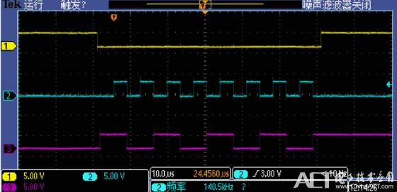
To make the image look nice, I only sent a 0xAA from STM32. I used SPI_BaudRatePrescaler_256, which is a 256 prescaler — 140.625KHz. The frequency captured by the oscilloscope is 140.5KHz, which is very close, and the data is 10101010, which is 0xAA. The next step is to use FPGA to mimic this timing.
Due to the large amount of content, please refer to the next part — Detailed Analysis of SPI Communication Between FPGA and STM32 (Part 2)
To be continued~