Word Count: 1800 Content Quality Index: ⭐⭐⭐⭐⭐
Modern CPUs are generally categorized into von Neumann architecture (also known as Princeton architecture) and Harvard architecture.
The von Neumann architecture refers to the X86 architecture, while the Harvard architecture refers to the ARM architecture. One is widely used in desktop environments (desktops/laptops/servers/workstations, etc.), while the other dominates the mobile field, as most handheld devices (tablets/phones) are based on it.
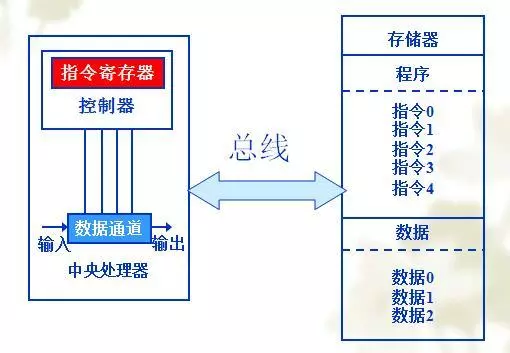
The diagram of the von Neumann architecture is as follows:
Characteristics of the Von Neumann Architecture:
A, both data and instructions are stored in the same memory area, using the same data bus for fetching instructions and data.
B, adopted by most early computers.
C, ARM7——the von Neumann architecture is simple, but slower. Instructions cannot fetch data simultaneously.
The von Neumann architecture, also known as Princeton architecture, is a memory structure that merges program instruction memory and data memory. The addresses for program instructions and data point to different physical locations in the same memory, thus the width of program instructions and data is the same, such as the Intel 8086 central processing unit, where both program instructions and data are 16 bits wide.
Processors based on the von Neumann architecture have the following characteristics:
2: Must have a controller;
3: Must have an arithmetic logic unit to perform arithmetic and logic operations;
4: Must have input and output devices for human-computer communication. Additionally, programs and data are stored uniformly and operate automatically under program control.
Other central processors from Intel.
MIPS Corporation’s MIPS processor.
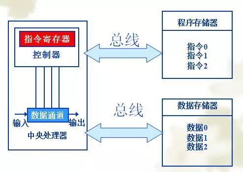
Diagram of the Harvard architecture
Structural Characteristics:
A, program memory and data memory are separate.
B, provides greater memory bandwidth, with each having its own bus.
C, suitable for digital signal processing.
D, most DSP systems are Harvard architecture.
E, ARM9 is Harvard architecture, allowing instruction fetch and data fetch to occur in the same cycle, improving speed. The Harvard architecture can be divided into three memory areas: program, data, and shared program and data.
The Harvard architecture is a parallel memory architecture, characterized by storing programs and data in different storage spaces, meaning program memory and data memory are two independent memories, each with its own addressing and access. Separating program instruction storage from data storage allows for different data widths for instructions and data.
The Harvard architecture fundamentally resolves conflicts between instruction fetch and data fetch. However, for accessing another operand, one must use the Enhanced Harvard architecture, such as TI’s approach, which splits the data area and adds another bus, or AD’s method, which uses instruction caches, allowing part of the instruction area to store some data.
The Harvard architecture has a critical weakness regarding dynamic program loading. Imagine reading a program from external storage and loading it into RAM. If this program is in data memory, we need a mechanism to transfer data memory back into program memory, which increases device complexity.
For multitasking operating systems, managing program memory is crucial, and just the mechanisms for page mapping in protected mode are already complex enough. If we also require separate management for programs and data, the complexity becomes too high. In such cases, the von Neumann architecture has a significant advantage.
The Relationship Between ARM and Harvard/Von Neumann
The Harvard architecture refers to the CPU fetching instructions from the cache, where instructions and data are not separated in main memory but are separated into two storage spaces when loaded into the cache, allowing the CPU to fetch both instructions and data simultaneously from the cache.
Thus, the ARM system CPU (except ARM7) appears as a von Neumann architecture externally, while internally it operates as a Harvard architecture.
Actual Chip Manufacturing
In reality, the vast majority of modern computers use what is known as “Modified Harvard Architecture,” where instructions and data share the same address space, but the caches are separate. This can be seen as a compromise between the two architectures.
In the real world, there are rarely purely conceptual frameworks, especially in practical applications. Most of what is found in textbooks are idealized models that help grasp the key points and essence of a concept, but achieving this idealized state is often difficult in practice.
The main difference between Harvard and von Neumann architectures lies in whether instructions and data are distinguished. In textbooks, these are two entirely different approaches.
However, in reality, instructions and data are together in memory. In the CPU’s cache, instruction cache and data cache are still distinguished, and during execution, instructions and data come from two different places. You can think of it as using the von Neumann model externally while employing the Harvard structure internally within the CPU.
Most DSPs do not have caches, thus they are directly Harvard architecture.
The Harvard structure is complex in design but highly efficient. The von Neumann structure is simpler but also slower. CPU manufacturers have added high-speed caches to improve processing speed. For the same reason, they have differentiated instruction caches from data caches. Sometimes, to solve practical problems, the distinction between these ideologies becomes less significant. Therefore, I personally believe that arguing over which structure is better is not very meaningful.
“Can One Learn Embedded Hardware and Software Well at the Same Time?”
“DJI Officially Announces Entry into Autonomous Driving! Smart Cars May Be Another Major Opportunity for Embedded Systems in the Next Decade!”
“iFLYTEK | 2021 Embedded Software Engineer Written Exam Questions”