Win a Backpack
How Hard Is It?
Give It a Try!
→_→

2016 Microcomputer and Applications Issue 3
Authors: He Peng, Hao Shaojie, Zhao Xinming
Abstract: High-speed real-time signal processing is one of the main features of broadband digital channelized reconnaissance receivers, and its performance determines the overall specifications of the reconnaissance receiver. To meet the real-time processing requirements of dense radar signals for broadband reconnaissance receivers, a parallel real-time signal processing platform based on FPGA and multiple multicore DSPs is designed, with chips interconnected via high-speed serial buses, using FPGA to schedule the multicore DSPs. This paper discusses the hardware implementation methods of the signal processing platform from aspects such as hardware system architecture, power supply, clock synchronization, and chip interconnection, and verifies the performance of the processing platform through practical applications, achieving the expected design goals.
0 Introduction
Broadband digital channelized reconnaissance receivers usually adopt a software radio design philosophy, using high-speed ADCs to directly sample RF or broadband intermediate frequency signals, implementing channelized reception and broadband signal processing using digital technology. With the development of high-speed ADCs and FPGA technology, digital channelized receiver systems can now achieve high-speed sampling of 1.8 Gb/s/12 bit and real-time channelization. To process such high-speed baseband signals with subsequent reconnaissance algorithms, a real-time parallel signal processing platform and efficient signal processing algorithms must be employed, where the signal processing platform must have efficient data transmission interfaces and sufficient floating-point computing capabilities.
This paper designs a signal processing platform based on Xilinx’s Kintex7 series FPGA and TI’s multicore DSP chip TMS320C6678 to address the real-time signal processing issues of broadband digital channelized receivers. It focuses on the hardware platform design implementation methods from system architecture, power supply, clock synchronization, chip interconnection, and provides experimental test results.
1 Overall Architecture Design
In the digital reconnaissance receiver system, the real-time signal processing platform receives channelized processed pulse signal data through high-speed interfaces, extracts signal frequency, pulse width, repetition frequency, intra-pulse modulation, and other characteristic parameters, and completes signal identification and classification through reconnaissance algorithms, finally outputting signal processing results. High-speed data transmission and parallel DSP algorithm implementation are key to this signal processing platform. To ensure interface bandwidth and signal processing performance, this paper constructs the hardware system based on high-performance FPGA and multiple multicore DSP chips, as shown in Figure 1.
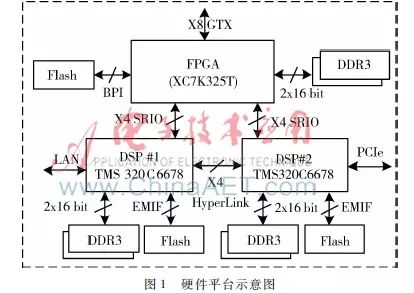
The FPGA selected is the Xilinx Kintex7 series chip, mainly used for high-speed data reception and scheduling of the DSP array. The FPGA receives IQ data packets sent from the channelization module through an x8 mode GTX interface, and then allocates the data to different DSP cores for characteristic parameter extraction, intra-pulse debugging recognition, signal classification, and other calculations according to a specific scheduling algorithm. The DSPs chosen are two TI TMS320C6678 chips, each containing 8 floating-point processor cores with a main frequency of 1.2 GHz, providing a total processing capability of 320 GFLOPS.
The hardware architecture adopts a flexible interconnection method, with the FPGA and two DSPs interconnected via high-speed serial bus (SRIO) interfaces. The two DSPs are interconnected via HyperLink interfaces, and the processed data can be uploaded to subsequent processing units via PCIe interfaces or gigabit Ethernet ports. The two DSPs can be configured to operate in parallel or serial modes. In parallel mode, the two DSPs alternately process different data frames; after receiving data to be processed, the FPGA distributes the data to idle DSP cores for processing via the SRIO interface. In serial mode, the two DSPs operate in a pipelined manner with a total of 16 cores, where each core completes a specific signal algorithm, passing data to the next core after computation. The working mode is flexibly chosen based on the density and characteristics of the pulse signals.
To reduce the system’s startup time, a parallel Flash chip is used to power up the FPGA and DSP, and the DSP boots via an external NOR Flash connected through the EMIF16 interface. The power-up loading of the two DSPs is completed independently, and once all processor cores are running, the FPGA schedules them uniformly for collaborative work.
2 Key Circuit Design Implementation
2.1 Power Supply System Design
In the high-performance signal processing platform designed in this paper, multiple high-speed digital signal processors and high-speed devices like DDR3 are used, with the working frequency of high-speed data lines exceeding 500 MHz and total power consumption exceeding 30 W. To ensure the stable operation of the hardware system, a reliable and efficient power supply system must be designed. This paper adopts a separate design scheme for the power supplies of FPGA and DSP to minimize the impact between power supplies and improve reliability. The entire circuit board uses a unified DC power supply, with a voltage range of +5.5 V to +15 V to adapt to different power supply environments. The power system scheme is shown in Figure 2.
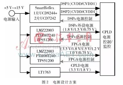
The power supply required by the FPGA and peripheral circuits is generated using a combination of LDO, DC-DC, and power modules based on different needs. The high current core power supply is generated through integrated power modules, while the power supply related to the GTX interface, which requires high power quality, is generated using linear regulators. The I/O power supply that requires high voltage is generated through DC-DC. The DSP power supply is mainly generated based on digital power management chips and integrated power modules, where the core power supply is generated by TI’s UCD series digital power management chips, consisting of a digital PWM control chip UCD9244 and two power driver chips UCD7242, providing two independent power outputs for the two TMS320C6678 chips. CVDD1 is fixed at 1.0 V, and CVDD ranges from 0.9 V to 1.1 V, which can be adjusted through the DSP’s VID. The configuration of UCD9244 can be achieved using Texas Instruments Fusion Digital Power Designer software.
To meet the strict power-up sequence requirements of the FPGA and DSP devices, this paper employs a CPLD chip to control the power-up sequence of each circuit unit and monitor the power supply health status. The power-up process is implemented in a closed-loop control manner, that is, after opening the first-level power supply and detecting its stable output, the next-level power supply is opened. If any power supply encounters an abnormal situation, the already opened power supplies are closed in reverse order of the power-up sequence, as shown in Figure 3.
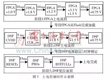
The power-up process is divided into three stages: FPGA power-up, DSP power-up, and DSP reset control. After the main power supply is turned on, the CPLD starts working, then controls the power-up of FPGA and its peripheral circuits in order. After detecting that the FPGA has completed loading the external Flash, it powers up the DSP and its peripheral circuits, sequentially turning on the core power supply, peripheral power supply, and clock enable. After detecting the clock lock signal, it enters the DSP reset control stage, sequentially outputting the DSP’s PORz, RESETFULLz, RESETz signals as required by the DSP device. When the normal working indication of the DSP is detected, the power-up is completed.
Through the refined design of the power supply system and accurate control of the power-up sequence, the impact of this signal processing platform on the entire system’s power supply can be minimized, reducing the instantaneous power supply capability requirements for the system. Gradual power-up can enhance the stability of the hardware of the signal processing platform and increase the lifespan of critical components, thus improving the reliability of the entire signal processing system.
2.2 Clock Circuit Design
In a multiprocessor system, clock synchronization is crucial. This design includes two TMS320C6678 processors, one FPGA chip, and multiple high-speed devices like DDR3, requiring multiple clock signals of different frequencies across the circuit board. Considering the load capacity of the clock source, impedance effects of branch lines, and noise affecting clock signal quality, this paper chooses a multi-channel clock generator plus clock buffers to produce various clock signals needed for the entire signal processing board, as shown in Figure 4.
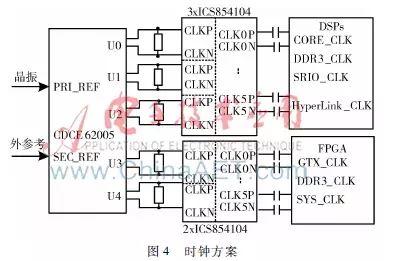
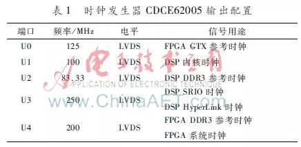
The multi-channel clock generator selected is TI’s dedicated clock chip CDCE62005, which is a high-performance clock generator and distributor with selectable reference input modes. Depending on the need, different reference clock schemes can be selected: when debugging the board, the high-stability crystal oscillator on the board is selected as input; when debugging in conjunction with the front-end channelization acquisition system, the synchronized clock signal provided by the channelization acquisition system is selected as the reference, ensuring complete synchronization of the clock with other circuit boards in the system. CDCE62005 can generate five independent differential clock outputs, with level formats selectable as LVPECL or LVDS, and output clock frequencies adjustable from 125 kHz to 1.5 GHz. Since the types and quantities of clocks needed by the FPGA and DSP exceed the output of the clock generator, the clock signals are classified and merged without increasing the number of clock generators, allowing the same frequency clock signals to use the same clock generator output port. Then, clock buffers SN65LVDS104 or SN65LVDS108 are used to expand a single signal to multiple paths, while performing level format conversion and increasing drive to provide to each circuit unit. According to the requirements of each circuit unit for clock signals, the configuration of the CDCE62005 output ports is shown in Table 1.
The configuration of CDCE62005 is implemented through CPLD programming, writing the user’s configuration parameters into the internal EEPROM memory via the device’s SPI interface. After power-up, the clock signal output or shutdown is controlled by the level of the PowerDown pin. When the PowerDown pin is high, CDCE62005 automatically calls the user configuration data to output the correct frequency. The internal EEPROM of CDCE62005 provides a lock function to protect the user’s configuration data, and after executing this command, the EEPROM cannot be changed again.
2.3 Interconnection Interface Design
Based on the characteristics of the FPGA and DSP devices in this design, as well as the bandwidth requirements for data transmission interfaces in the signal processing platform, a serial high-speed bus is selected for interconnection between chips. The pulse signal data to be processed is transmitted to the FPGA of the signal processing board via the x8 mode GTX interface; the FPGA connects to the two DSPs via two sets of GTX interfaces, using the SRIO protocol for data transmission; the DSPs communicate via the HyperLink interface; and the signal processing results are reported via the PCIe or gigabit Ethernet interfaces of the DSP chips.
2.3.1 FPGA and DSP Interconnection Design
SRIO (Serial RapidIO) is an open, packet-switched high-speed serial standard for interconnection between embedded system chips and boards. The GTX interface of the Kintex7 series FPGA can be configured for the SRIO protocol, allowing seamless connection with the TMS320C6678’s SRIO interface. The SRIO protocol in the FPGA is implemented by invoking the IP core provided by Xilinx, using the Core generator in ISE software to call the Serial RapidIO Gen IP core, configure the relevant parameters, generate the IP core module, and then create two FIFOs in the FPGA to store the data to be sent and received, respectively, controlling the IP core through a finite state machine.
The configuration of SRIO on the TMS320C6678 side can be achieved by calling the relevant API functions in TI’s CSL library. It is important to note that the endpoint ID numbers defined in the FPGA and DSP must be consistent; otherwise, communication will not be possible. During the debugging of the SRIO communication interface, the ChipScope is used in the FPGA to check the status of relevant signals to determine whether SRIO communication is successful. First, check the status of the SRIO IP core output indication signal clk_lock; if this signal is high, it indicates that a clock has entered the SRIO core and is locked. After the clock is locked, check whether the clocks on both the FPGA and DSP sides are correct and whether the transmission rates match. When the SRIO IP core indication signal link_initialized on the FPGA side is pulled high, it indicates that communication has been established. At this point, a loopback test for SRIO can be performed, and if both sides pass the loopback test, it indicates that the physical link has been established, allowing data transmission and interface bandwidth testing to proceed.
2.3.2 DSP Interconnection Design
The HyperLink bus is an efficient interconnection scheme for embedded applications with a low pin count, where data transmission is entirely implemented by hardware without processor involvement. In this design, the two TMS320C6678s are interconnected via the HyperLink interface, with each DSP providing four SerDes channels for HyperLink, supporting a maximum transmission rate of 12.5 Gb/s and using 8b9b encoding, with a data throughput of 12.5×4×(8/9)=44.5 Gb/s. TI provides a rich set of HyperLink API functions in the CSL library, and in the CCS development software, the relevant API functions are called to configure the HyperLink interface, using memory mapping to map the memory space of DSP2 onto DSP1, allowing DSP1 to access DSP2’s memory space as if it were its own local space, facilitating data exchange.
3 Test Verification
To test the data transmission and real-time processing capabilities of the signal processing platform, the following experiments were conducted: The FPGA reads a frame of pulse signal data from the front-end processing system via the GTX interface, with 512-point IQ data totaling 512×32×2=32,768 bits. The DSP reads the data from the FPGA into memory via the SRIO interface and starts multiple cores to perform intra-pulse modulation characteristic analysis simultaneously. The GTX of the FPGA operates in 8x mode at a baud rate of 10 Gb/s, while the DSP’s SRIO interface operates in 4x mode at a baud rate of 6.25 Gb/s, with the DSP working at a main frequency of 1.2 GHz. The runtime record function of the CCS software is used to test the time consumed for the entire processing flow, as shown in Figure 5.
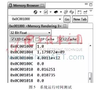
As shown in Figure 5, the time taken from the FPGA starting to read data until the data enters the DSP memory is 0.016251 ms, and the time taken by the DSP to perform intra-pulse modulation characteristic analysis is 0.010375 ms, with a total processing time of about 26 μs for a frame of pulse signal.
4 Conclusion
This paper introduces a method for implementing a high-speed real-time signal processing platform from the perspective of hardware design, constructing a system based on Xilinx’s Kintex7 series FPGA and TI’s multicore DSP chip TMS320C6678. It details the design and testing of the power circuit, clock circuit, and chip interconnection scheme. High-speed serial interfaces are used to achieve data exchange between chips, and parallel computation based on multicore DSPs enhances computational efficiency, addressing the bottleneck of massive data transmission and real-time signal processing speed in broadband reconnaissance receiver systems, thus improving the adaptability of the reconnaissance receiver to dense signal environments. This signal processing platform features large data transmission bandwidth, strong parallel processing capability, and high reliability, meeting the needs of practical engineering applications.
References
[1] Gong Shixian, Wei Xizhang, Li Xiang, et al. Overview of Broadband Digital Channelized Receivers. Journal of Electronics, 2013, 41(5):118-122.
[2] Hao Shaojie, He Peng, Zhu Weifeng. Design and Implementation of Dual-Channel High-Speed Data Acquisition and Processing Platform. Computer Measurement and Control, 2015, 23(7):35-39.
[3] Wu Bin, Yang Shenhua, Yang Na, et al. Design of Shipborne Radar Information Acquisition Card Based on DSP and FPGA. Microcomputer and Applications, 2015, 34(13):31-34.
[4] Wu Minjie, Feng Qi, Yuan Naichang. Power Design of TMS320C6678 DSP. Electronic Design Engineering, 2012, 20(6):46-49.
[5] Dong Yuanwen, Zhang Yongjun, Gao Xiaoliang, et al. Distributed Communication System Based on TMS320C6678 Multicore DSP. Microcomputer and Applications, 2014, 33(13):74-76.
[6] Li Xin, Jiang Ming. Design of High-Speed Real-Time Signal Processing System Based on Multicore DSP. Optical Technology, 2012, 38(1):55-60.
[7] SPRUGW1. KeyStone Architecture Serial RapidIO (SRIO) User Guide. Texas Instruments, 2010.
[8] SPRUGW8. KeyStone Architecture HyperLink User Guide. Texas Instruments, 2010.